Power control using the linear region of an active device, such as a MOSFET, is not an efficient option. However if the range of power control is restricted to the lower or upper end of the range, using the linear region is not a bad choice.
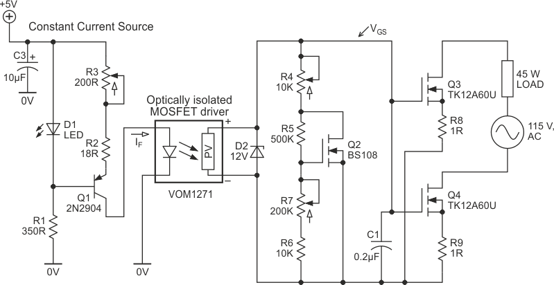
For instance, if we wish to control the power of a 45 W soldering iron between 35 W & 45 W, an active device will dissipate between about 4 W & 0.1 W. With this in mind, the circuit shown in Figure 1 has been developed.
 |
|
| Figure 1. | AC linear power control circuit. |
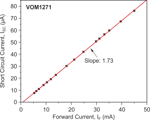
A simple current source is used to drive a VOM1271 photovoltaic (PV) coupler. The output voltage of the VOM1271 can be a maximum of 8.4 V. Figure 2 shows the relationship between the input forward (IF) current with the output short circuit current (ISC) – essentially linear. Photovoltaic output behaves like a constant current source until it nears the open circuit voltage (~8 V). This output voltage can be utilized to drive a MOSFET with threshold voltage (VTH) less than 8 V.
 |
|
| Figure 2. | Transfer characteristics of a photovoltaic coupler. |
A difficulty with MOSFETs in linear mode is that even in the same batch of devices, gate-source threshold voltages vary. Just after the threshold, drain current increases rapidly with little change in VGS [1]. MOSFET Q2 at the output of the PV coupler is biased in such a way that the output voltage to be applied to Q3 & Q4 gates (VGS) changes in accordance with the transconductance of Q3 and Q4.
 |
|
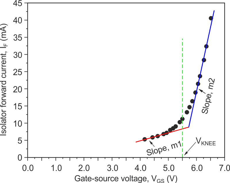
| Figure 3. | VOM1271 forward current vs. gate-source voltage. |
Figure 3 shows the VOM1271 forward current (IF) vs. VGS relationship. With a little IF, VGS reaches the knee voltage (VKNEE) with a slope m1. This slope is approximately proportional to
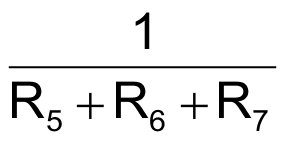
as R5 + R6 + R7 >> R4. We can adjust R7 so that VKNEE matches close to the threshold voltage of Q3 and Q4 (about 4 V to 5 V). After the knee, voltage VGS changes more slowly with IF, with a steeper slope m2, similar to the VGS vs. ID curve of MOSFETs. Slope m2 is controlled by trimmer R4 (m2 ∝ 1/R4).
Q3 and Q4 are connected as shown in the schematic to conduct AC. A 45 W soldering iron is used as the load to be controlled by the circuit. As the threshold voltages of Q3 and Q4 may vary, 1 Ω resistors R8 and R9 are used to partly counteract this. As both Q3 and Q4 are getting the same gate voltage, higher load current causes higher voltage drop, which tends to reduce ID. The values of R8 and R9 should be chosen considering the AC load; the larger the load, the lower the values.
The voltage waveform across the load is shown in Figure 4 at various power levels. A little imbalance between the positive and negative halves is seen, especially at the lower power, because of the difference in VTH. The waveforms are much like a truncated sinusoidal wave. However, this distortion is less likely to generate RFI compared to conventional triac-controlled waveforms.
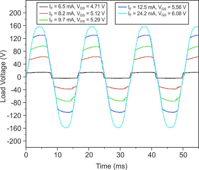 |
|
| Figure 4. | Voltage waveforms across the load at various power levels. |
Though a constant current source is used here for power control, it can be replaced by any other control sources. The optical isolation will keep the control sources safe from the AC. Though this circuit is used here for AC power control, it can be used for DC as well.