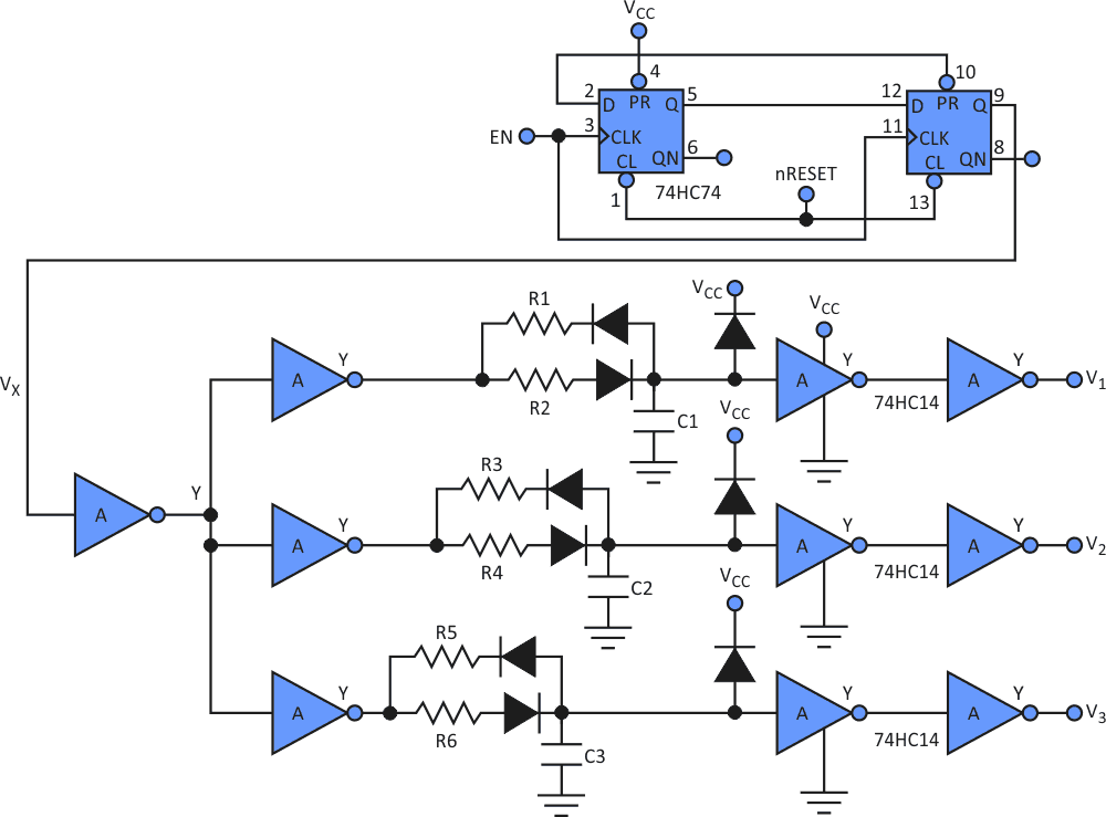
Many graphic (passive/active (TFT)) LCDs require multiple positive and negative supply voltages. At “power on” and “power off,” these bias voltages must be sequenced properly, along with the LCD’s data and control signals, to prevent damage to the LCDs. Figure 1 shows a circuit that can provide the needed sequencing.
 |
|
| Figure 1. | This circuit sequences three different delays to bias voltages V1, V2, and V3 so that an LCD can be powered up and powered down properly. |
The inverters are 74HC14 Schmitt types. The resistor-diode-capacitor networks form the delay circuits, with the diodes enabling different charging and discharging time constants. In the circuit, three programmable delay stages generate V1, V2, and V3. Additional stages are possible for LCDs that require more than three supply voltages.
A supervisory IC generates the Power On Reset signal (active low nRESET), which disables all voltages and data/control signals to the LCD. At Power On Reset, the 74HC74 D flip-flops output and VX is at logic low level. (Two flip-flops are used to prevent any Power On transition on EN from clocking the flip-flops.) Also, the capacitors are uncharged, and V1, V2, and V3 = 0 V. This is the bias voltage’s Power Off state. A bus switch is used to disable the data and control signals to the LCD.
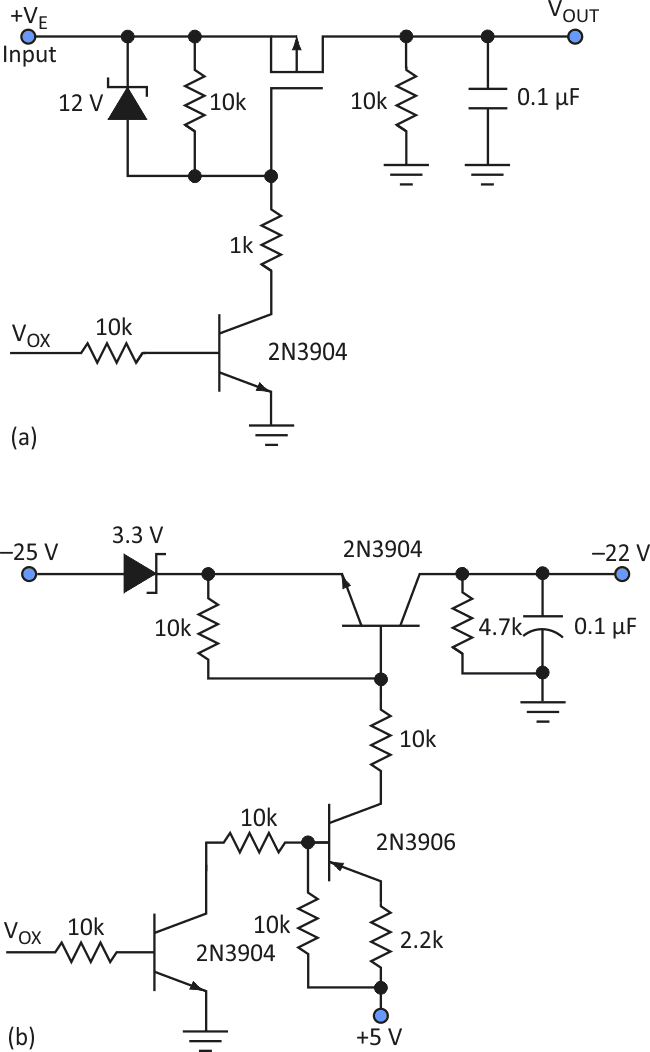
The EN signal should appear only after the LCD controller is initialized and the signals are active. (EN can also be connected to VSYNC, so that when the LCD controller is initialized, LCD power is auto-enabled.) One STN passive-type LCD requires the power-on sequence to be: VCC, then LCD data/control signals, then 22-V bias (with greater than 20 ms delay in between). In this example, V1 controls VCC to the LCD using a positive voltage switch (Fig. 2a), V2 controls the bus switch, and V3 controls the 22-V bias using the negative voltage switch (Fig. 2b). The negative switch is designed specifically for 22-V bias switching. The MOSFET in the positive switch should have a logic-level threshold. Both switches use active-high power Enable signals.
 |
|
| Figure 2. | V1 controls VCC to the LCD through the positive voltage switch (a), while V3 controls the –22-V bias through the negative control switch (b). |
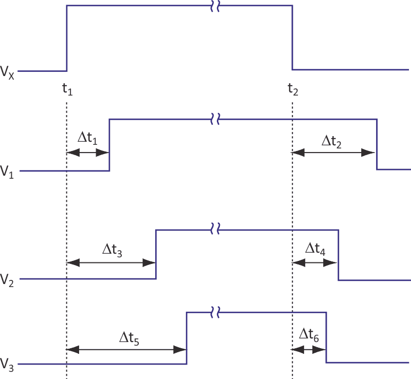
When the supervisory processor pulses EN twice, V1, V2, and V3 go high after the delay determined by time constants R2C1 (Δt1), R4C2 (Δt3), and R6C3 (Δt5), respectively (Fig. 3). The diode connected to negative VCC discharges the capacitor if VCC dies off fast at Power Off. When power goes down, nRESET goes low (before the power fully goes down), and C1, C2, and C3 discharge with different time constants: R1C1 (Δt2), R3C2 (Δt4), and R5C3 (Δt6), respectively.
 |
|
| Figure 3. | V1 controls VCC to the LCD through the positive voltage switch (a), while V3 controls the –22-V bias through the negative control switch (b). |
Note that by adjusting the time constants, the 22-V bias is enabled only when power and data signals are applied, and data signals are enabled only after VCC is applied. The resistance could be 10 to 47 kΩ, and the capacitors can be 0.1 to 0.47 µF, X7R types.
The data and control signals can be controlled by a bus switch, such as the CBT, FST, or PI5C families, or their 3.3-V counterparts. Or, they can be controlled with 8, 20, or 24-bit wide switches like the xxx245, 16210, and 16211.