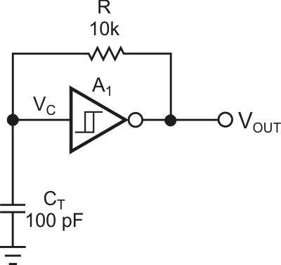
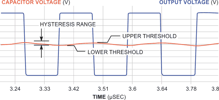
Many designs exist for logic-based astable multivibrators, one of the simplest being an RC feedback loop around a single inverting Schmitt trigger inverter (Figure 1). The output charges the capacitor to the upper switching threshold, at which point the output switches to its opposite state, the threshold switches to a different value, and the capacitor’s charging current reverses direction. When the capacitor’s voltage crosses the lower threshold, the output and threshold both toggle back to their original values, and the process repeats. The timing depends on both the RC time constant and the hysteresis resulting from the spread between the two threshold values (Figure 2). Unfortunately, although inverter manufacturers specify the hysteresis voltages in their data sheets, the devices have a fairly large range. In addition, they likely have some temperature dependence. These uncertainties make it difficult to design the circuit to have a predictable oscillating frequency.
 |
|
| Figure 1. | A basic astable multivibrator uses a Schmitt trigger and an RC network. |
 |
|
| Figure 2. | A part’s hysteresis, in large part, determines switching thresholds. |
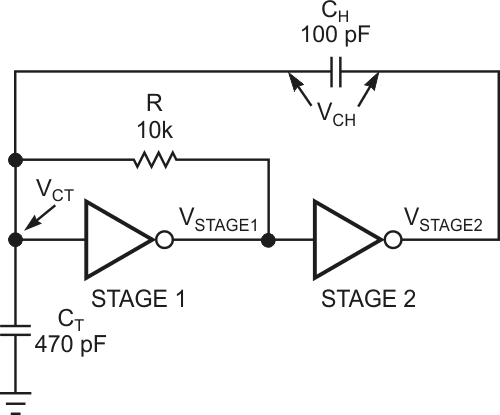
A simple inverter, without the hysteresis to let it overshoot the nominal threshold, charges the capacitor to the threshold voltage and stops in its narrow linear region. At this point, the negative feedback from the inverting output to the input regulates the output to the threshold voltage. Adding another inverting stage injects hysteresis of a different form by means of positive feedback, which external passive parts determine (Figure 3).
 |
|
| Figure 3. | The addition of a positive-feedback stage provides hysteresis to a simple inverter stage. |
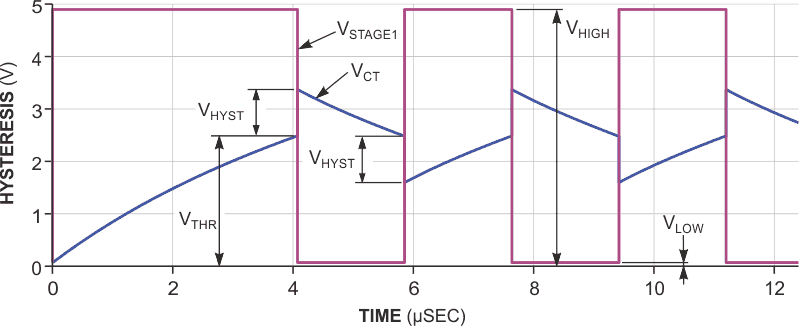
Whenever Stage 1 crosses its threshold, the extra Stage 2 injects an additional charge through a feedback capacitor to make the timing capacitor’s voltage jump past the threshold. The RC charging current reverses direction to get back to the threshold voltage. When it gets there, the hysteresis-injection circuit again jumps the voltage past the target so that the RC timing circuit must again reverse the charging current to seek the threshold voltage (Figure 4). This process continues endlessly at a fairly predictable rate. In the equations, CT is the timing capacitor, CH is the hysteresis capacitor, VTHR is the threshold voltage, VLOW is the low output voltage, and VHIGH is the high output voltage.
 |
|
| Figure 4. | Hysteresis results from a charge burst from Stage 2 that jumps the timing-capacitor voltage past the switching threshold by a known, fixed amount. |
You can view the hysteresis-overshoot voltage, VHYST, as the result of a capacitive voltage divider that timing capacitor CT and hysteresis capacitor CH form. When Stage 1 toggles Stage 2, its output jumps from a low value to a high value or from a high value to a low value by an amount of VHIGH – VLOW, and the voltage of the timing capacitor jumps by
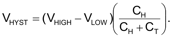
Second, the voltage of the timing capacitor relaxes back toward Stage 1’s output voltage by drawing current through both the timing capacitor and the hysteresis capacitor.
Thus, the relaxation time constant is R(CT + CH) and the relaxation voltage is either
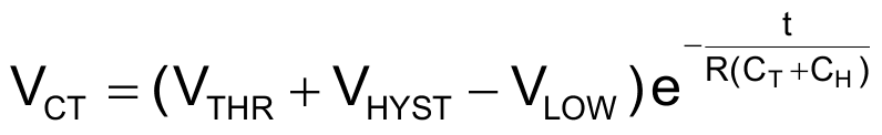
or
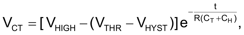
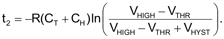
depending on which half-cycle is occurring. You calculate the time from VTHR + VHYST back to VTHR as
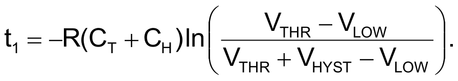
For the other half-cycle,
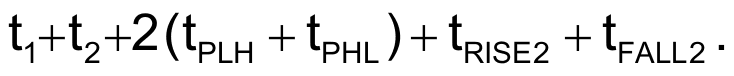
You should add the total propagation time (tPLH + tPHL) through stages 1 and 2 to the total period. Unless you want the circuit to operate at its maximum frequency, these propagation times become insignificant. The period prediction then depends only on passive-component values and their tolerances, temperature, and aging coefficients. The series combination of CT and CH, however, presents a capacitive load to Stage 2. This load affects Stage 2’s rise and fall times, the sum of which you must add to the total period, T.
In the case of CMOS parts, such as the 74VHC04, rise and fall times depend on the output resistance of the part as well as on the external components. If you model the Stage 2 output as an RC circuit, you can estimate the 10 to 90% exponential rise and fall times as
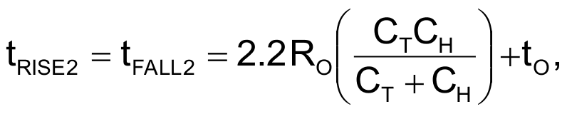
where tRISE2 is the rise time, tFALL2 is the fall time, RO is the output resistance of the part – 30 Ω for the 74VHC04 – and tO is the no-load rise time – in this case, 4.5 nsec for the VHC04. Thus, the total period is
Also note that the timing depends on inverter output voltages and the location of the threshold voltage within that range. For example, a CMOS part whose outputs are close to the power rails is more predictable than a TTL (transistor-transistor-logic) part, and a 74HC part with a midpoint threshold voltage has a more symmetric output than an HCT part whose threshold voltage is offset for TTL interfacing.
For higher frequencies, you must use smaller resistor values, smaller timing-capacitor values, or both. For predictable results, the value of the timing capacitor should be no less than 10 times the inverter’s input capacitance, which ranges from 3 to 10 pF for a typical CMOS, and R should not be so low that it significantly loads down the output. As a precaution, the value of the hysteresis capacitor should not exceed that of the timing capacitor so that it does not exceed the maximum input voltage on Stage 1. If the value of the hysteresis capacitor were much greater than that of the timing capacitor, then the threshold voltage and the hysteresis voltage would approach 7.5 and –2.5 V, respectively. The 74VHC04 part proves the calculations using 5% resistors and 20% capacitors.
| Table 1 | 74VHC04 results | ||||||||||||||||||||||||||||||||||||||||||||||||||||
|
|||||||||||||||||||||||||||||||||||||||||||||||||||||
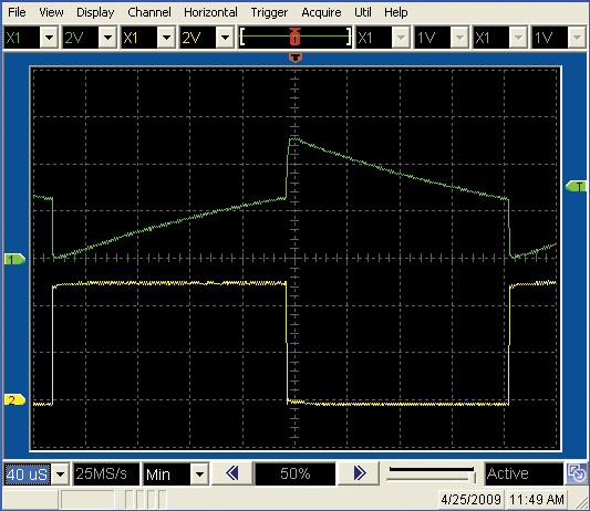
Table 1 summarizes the results, which are within the component tolerances. Figure 5 shows a typical input and output plot.
 |
|
| Figure 5. | The circuit is well-behaved at low frequencies. |