This Design Idea describes a simple way to form a reliable astable or monostable multivibrator from a set/reset latch. You may find it useful because it lets you minimize the number of standard digital ICs your design requires when absolute precision isn't an issue. You can use a set/reset latch either with active-low or active-high inputs, which you can build with two NAND or NOR logic gates. You can also use integrated set/reset latches or any type of flip-flop that comes with asynchronous preset and clear inputs because they have the same function as the set/reset inputs when the clock and data inputs are grounded. This method functions only with CMOS-logic families that offer the benefits of high input impedance; a quasi-ideal voltage-transfer characteristic with a threshold voltage, VTH, typically equal to the drain-to-drain voltage, VDD, divided by two; and low power consumption. This concept has undergone testing with a 74HC00 quad NAND, a 74HC02 quad NOR, a CD4001 quad NOR, a CD4011 quad NAND, and a CD4013 dual-D-type flip-flop.
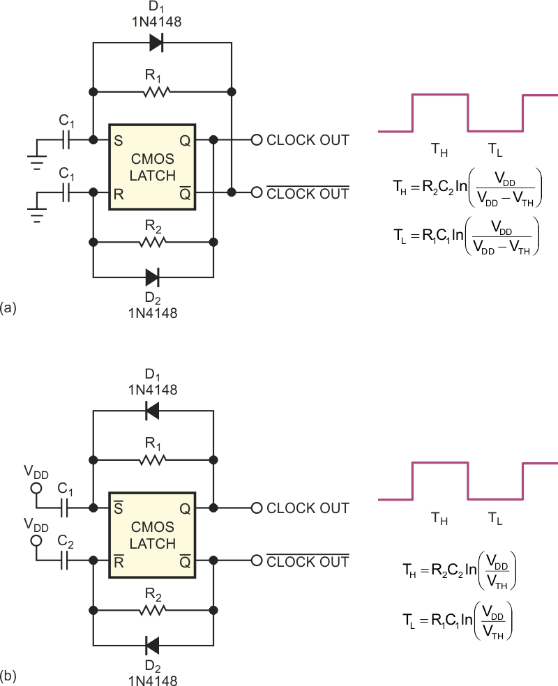
Connecting two RC networks between the complementary outputs Q and /Q and set and reset inputs enables astable operation (Figure 1). Due to complementary outputs, the circuit has no stable state, and it toggles continuously, generating an output clock.
 |
|
| Figure 1. | Capacitors that connect to ground or VDD depend on active-high (a) or active-low (b) inputs. |
The time constants R2C2 and R1C1 set the high and low time periods, TH and TL, respectively, and also the duty cycle. Diodes D1 and D2 quickly discharge capacitors C1 and C2 so that, on the next cycle, they will recharge from 0 V.
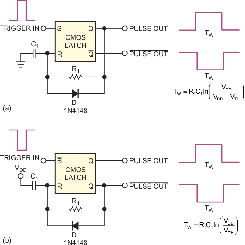
In monostable mode, connect one RC network (Figure 2), depending whether you need a positive-pulse or a negative-pulse trigger. When an input trigger pulse occurs, it sets the output pulse, TW, which remains in this state until the RC network activates the reset pin. The RC time constant sets the output-pulse width. For correct operation, the trigger pulse must be shorter than the output pulse. Diode D1 reduces recovery time.
 |
|
| Figure 2. | The leading edge of the trigger pulse depends on active-high (a) or active-low (b) inputs. |
The threshold voltage has the typical value VDD/2, but it may change from 0.33 to 0.67 of VDD for the CD4000 CMOS family. The parameters of the generated output signals of the circuits in figure 1 and figure 2 present variations from unit to unit as a function of threshold-voltage shift. On the other hand, the threshold voltage presents good stability with supply voltage and temperature variations.
For best accuracy, the timing capacitors for both astable and monostable circuits should be nonpolarized, have low leakage, and be much larger than the inherent stray capacitance in the circuit, and the timing resistors for both astable and monostable circuits must be much larger than the CMOS on-resistance in series with them, which typically is hundreds of ohms. In addition, you must decouple the supply voltage for safety to prevent voltage spikes, which may disturb the circuits.