Circuits sometimes need a gain-of-one buffer to lower output impedance and prevent the load from interfering with the previous stage. For an application involving a 1.5-MHz, low-power transmitter and antenna, a BUF634 buffer IC would work, but a discrete transistor buffer may be more convenient and less expensive than the IC.
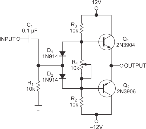
Figure 1 shows the classic design of such a buffer. This circuit can drive a load as low as 200 Ω with a peak output voltage of 2 V. The maximum collector current of the transistors limits the output. You can use larger output transistors if your application requires more output current. Trimmer resistor R4 across the diodes is, however, a relatively expensive part, and you must adjust it to produce the correct bias current for Class AB operation. The adjustment is likely to drift over time.
 |
|
| Figure 1. | A typical buffer can drive loads as low as 200 Ω. |
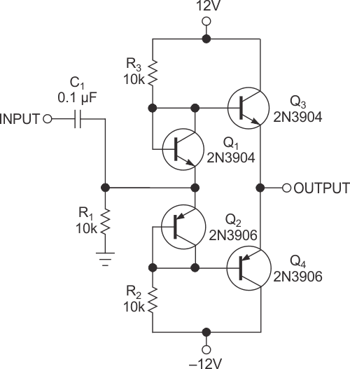
A simpler circuit, such as the one in Figure 2, uses current-mirror transistors Q1 and Q2 instead of diodes. Resistors R2 and R3 set the zero-signal bias current in the bias-transistor circuits. The current-mirror effect causes the current in the output transistors to be nearly equal to the current in the bias transistors – approximately 1.2 mA in this case. Because the current-gain-bandwidth product of the 2N3904 and 2N3906 transistors is 300 MHz, this circuit should work at 100 MHz or higher frequencies.
 |
|
| Figure 2. | Current-mirror transistors replace the diodes in Figure 1. |
At these frequencies, however, the circuit layout may be critical, and the slew rate, which is unknown, may limit usefulness. The offset of the circuit is approximately 0.1 V, which is not a problem for this application because the circuit uses capacitive coupling through C1. If you use the buffer in the feedback loop of an op amp, the op amp can null the offset.
 |
|
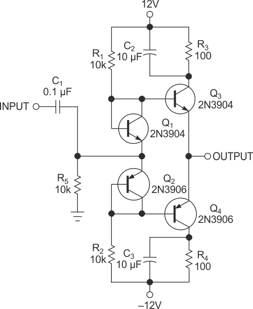
| Figure 3. | Resistors R3 and R4 limit the output current. |
You may want to monitor the current in the output transistors, so the circuit in Figure 3 adds 100 Ω resistors R3 and R4 and 10-μF bypass capacitors C2 and C3 in the collectors of output transistors Q3 and Q4. The voltage across these resistors reveals the collector currents, which are nearly equal in the two output transistors, and is close to the value that the values of R1 and R2 predicted.