Most current microprocessors, DSPs, and field-programmable gate arrays integrate hardware and software resources that support either or both of two common interface standards – SPI (serial-peripheral interface) and I2C (inter-IC)/SMBus. Both two-wire-interface standards suffer from a few crucial disadvantages. For example, I2C's throughput rates are 100 kbps, 400 kbps, or 3.4 Mbps in standard-, fast-, and high-speed modes, respectively, and can thus restrain a fast peripheral data converter's sample rate. Excluding framing and overhead bits, a 100k-sample/sec, 12-bit ADC must transfer at least 1.2 Mbps over the interface, a rate that only I2C's high-speed mode supports. Many processors and controllers currently offer no I2C high-speed mode and thus would be unable to support a fast data converter.
One of I2C's major benefits reduces the number of host-to-target interconnections. Using only two wires plus ground, the host controller can address the target device and exchange data, whereas SPI requires three wires – data, clock, and chip-selection – plus ground. Multiple SPI-target devices can share data and clock lines, but each device requires its own dedicated chip-selection line.
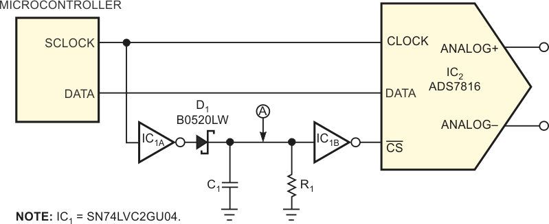
Given the perpetual demand for higher sample rates and resolution, I2C's limited speed may restrict its use in some applications and instead force designers to select SPI. However, SPI requires an additional I/O pin on the host controller. In situations in which extra pins are unavailable but the application requires a fast SPI-bus converter, you can apply the technique in Figure 1.
 |
||
| Figure 1. | Two inverters and a few components can substitute for an SPI ADC’s chip-select line. |
|
For example, Texas Instruments' ADS7816 comprises a 200k-sample/sec, 12-bit-sampling ADC that requires a bit rate of 3 M samples/sec to sample continuously at a 200k-sample/sec rate. Selecting the ADS7816 's active-low /CS (chip-select) pin initiates a conversion cycle. After toggling and holding /CS low during the data transfer, /CS returns high after transferring the data completes the process.
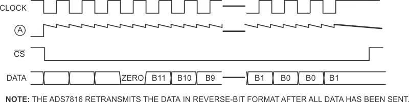
When the clock line initially goes low, it also asserts /CS to a low state. The time constant of the peak detector comprising D1, R1, and C1 ensures that /CS does not go high until the clock line remains high for more than one clock cycle (Figure 2). Although the clock line toggles and retrieves data from IC2, /CS remains asserted low, and, upon completion of retrieval, the clock line goes high, and /CS follows, readying the circuit for another conversion cycle.
 |
||
| Figure 2. | An SPI-clock waveform (top trace) evokes data (bottom trace), and peak detection of the clock (the waveform at Point A in Figure 1) yields a signal (next-to-bottom trace) that mimics the chip-selection line’s behavior. |
|
Because C1 must discharge at the end of a conversion cycle, the controller should delay the start of the next conversion cycle until C1 fully discharges. Careful choice of R1 and C1 minimizes the delay to a minimum of three clock cycles. In addition, the voltage across C1 must not fall below inverter IC1B's input threshold before the next clock pulse arrives to refresh the capacitor's voltage. Inverter IC1A's output voltage and current capabilities affect C1's recharge time, and R1 and IC1B's input impedance affect the discharge time. To ensure a robust design, include components' tolerances and temperature coefficients along with variations of logic-input and -output thresholds.