The synchronous oscillator (SO) and the coherent phase-locked synchronous oscillator (CPSO) are universal multifunctional networks that track, synchronize, and amplify as much as 80 dB; improve SNR by as much as 70 dB; and modulate AM, FM, and FSK signals. You can also use these networks as ADCs, sampling networks, and dividers that divide by rational integer numbers, such as 3/4, 5/7, and 7/8. Suitable applications include wideband spread-spectrum communications and binary-phase-shift-keying (BPSK) and quadrature-phase-shift-keying (QPSK) generation. A CPSO retains all the properties of the SO and provides zero phase error.
 |
|
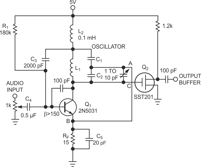
| Figure 1. | A single-stage synchronous oscillator converts audio or video to FM. |
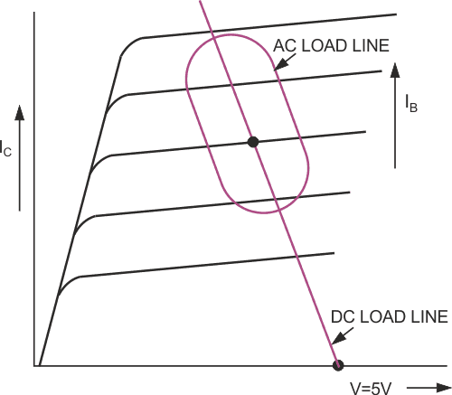
One SO application area is the conversion of audio and video to FM in a single process. Figure 1 shows a simple, one-stage SO oscillating at 94 MHz. This frequency is a good choice for testing the audio-to-FM conversion on an FM broadcast receiver. The audio or video input to this SO should not exceed –5 dBm; any signal above this level may induce amplitude modulation. C4’s decoupling capacitor passes the audio or video to the SO and eliminates dc bias at the input. R1 biases the SO. Because the oscillator's load is a combination of resistance, inductance, and capacitance, the load line is a combination of a straight line and an ellipse (Figure 2). The linear load line indicates the dc bias, and you must locate the load line away from the nonlinear characteristics of the transistor.
 |
|
| Figure 2. | The load line is a combination of a straight line and an ellipse. |
C3 and the connection between points A and B each provide positive feedback. High positive feedback is essential to the optimum operation of the SO. The value of C3 should range from 2000 to 5000 pF. RF in parallel with C5 has numerous functions. The presence of this network allows positive feedback within the SO, but looking from the input, RF and C5 also provide negative feedback. This negative feedback adds frequency stability. Finally, RF and C5 divert the input audio or video to the oscillator, not to ground. RF and C5 are approximately 15 Ω and 20 pF, respectively, and these values depend on the β of the transistor. L2 is an RF choke that diverts the collector feedback to the base of the transistor. You should tune the tank circuit, which comprises L1, C1, and C2, to approximately 95 MHz to be within the FM broadcast band. A 2N5031 for Q1 works well for this application because it has high gain and low noise; any other transistor with the same characteristics is suitable. A 2- or 3-in. long wire attaches to the output and acts as an antenna.
The conversion from audio or video to FM takes place in the internal base-emitter junction capacitor by its parametric action, and the changes of the junction capacitor due to audio-to-video variations modulates the oscillations to provide an audio- or video-to-FM conversion.
The SO also has high input-signal sensitivity and high noise rejection. It can detect signals as low as –100 dBm and signals with SNRs as low as –40 dB. For a PLL, these performance numbers are –25 dBm and 3 dB, respectively. The SO is frequency-stable and has low phase jitter because the tank circuit has a high Q that can reach 3×10⁶. The SO has three independent internal filters. With a 200-Hz noise-rejection filter, the SO exhibits a data bandwidth or tracking range of several megahertz. For input signals with high noise, a two-transistor cascoded SO is preferable.
The output buffer, Q2, provides protection between the oscillator and the output world. However, if you want to simplify the circuit, you can remove Q2 and its 1.2-kΩ pullup resistor and connect the 100-pF capacitor at the output directly to Point C.