Engineers often face difficult trade-offs when voltage regulators can encounter high-voltage transients that are well above normal input-supply operating ranges. This situation is common in automotive applications in which high-voltage transients from an alternator load dump can produce transients of 36 to 75 V for durations as long as 400 msec. Designers must choose between a regulator that can withstand such maximum input voltage or use an input-protection scheme. The simple circuit in this Design Idea provides a highly cost-effective method for clamping an input voltage from a battery input with transients as high as 50 V to take advantage of a 20 V, 3-MHz regulator. With this circuit, your design can achieve a small total footprint with relatively low cost because of the 3-MHz operation along with lower voltage components than might otherwise be necessary to withstand 50 V.
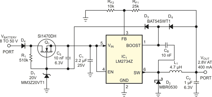
Input-protection components consist of Q1, R1, D1, C5, and one-half of D2 (Figure 1). At start-up, N-channel MOSFET Q1’s source is at ground potential and turns on when R1 applies the battery voltage to the gate. Once the input voltage is above the minimum of 2.74 V on IC1, the LM2734Z regulator starts switching, which charges the bootstrap circuit comprising D3, D4, and CB. This bootstrap voltage of approximately VOUT – VFD (forward-voltage drop) of D3 then transfers to the gate source of Q1. Capacitor C5 then maintains gate drive during the bootstrap diode’s off times.
 |
|
| Figure 1. | The N-channel MOSFET and zener diode protect the switching regulator against transient voltages as high as 50 V in automotive applications. |
Under normal operating conditions, for example, the battery voltage is 8 to 18 V, D1 does not limit conduction of Q1, and the gate voltage tracks approximately 2.5 V above the input-supply voltage for a low voltage drop from the battery voltage to the input voltage of the LM2734Z. However, when the input voltage increases above the threshold that D1 sets, the input voltage to the LM2734Z regulates to the zener voltage (VZ) of D1 minus the threshold voltage of Q1, or approximately 20 – 2 V = 18 V, well below the 24 V absolute maximum of the LM2734Z. Selecting Q1 requires careful consideration of maximum input voltage, gate-to-source-voltage threshold, and power dissipation under both steady-state and thermal-transient conditions.
Q1, the SI1470DN N-channel MOSFET, provides 50 V protection with a drain-to-source voltage (VDS) of 30 V + 20 V (zener diode D1 voltage), has an on-resistance of 95 mΩ at a gate-to-source voltage of 2.5 V, and comes in a thermally efficient SC70-6 package. For some applications, the regulator’s output voltage may be insufficient to fully turn on the selected protection MOSFET, so you can increase the bootstrap voltage with a separate zener reference, as the LM2734Z’s data sheet shows.