Testing and measuring an IC’s or circuit’s performance with regard to power transients is a tricky task to accomplish without some specialized equipment. Not only does the input voltage source need to change in a controlled manner, but it must be able to source enough current to slew the input capacitance and power the circuits under test.
One way to generate positive line transients, e.g., 4 V to 12 V, relatively easily is to use a couple of diodes to switch between two power supplies. While easy, this method offers no way to control the dV/dt of the input voltage. Negative line transients are much more difficult to achieve as many benchtop power supplies cannot sink current from the capacitors to slew their voltage negatively. Trying to hang a current source across the capacitors to sink current from them during negative slewing and properly switch in power supplies without damaging them is easier said than done. However, should an application require a pulsed input voltage or both positive and negative line transients, neither of these methods will work.
Not long ago, I found myself in exactly that situation while testing a new IC with built-in input over-voltage (OV) and under-voltage (UV) protection. Very specific VIN waveforms were required in order to prove the functionality of these features. If VIN went above the OV or below the UV threshold for longer than the datasheet time, the chip should shut down and require a restart. If however the input voltage to the IC recovered and went back inside the allowable limits inside of that time, the part should continue to function normally and would not require a restart. While I could test the OV and UV shut-down features easily enough, none of my usual tricks would work to test the self-recovery function as I had no way to slew the input voltage up and down fast enough. With a recovery time on the order of tens of microseconds, and having to power both the IC itself and slew the input decoupling capacitance of 20 µF, simply using a function generator was out of the question.
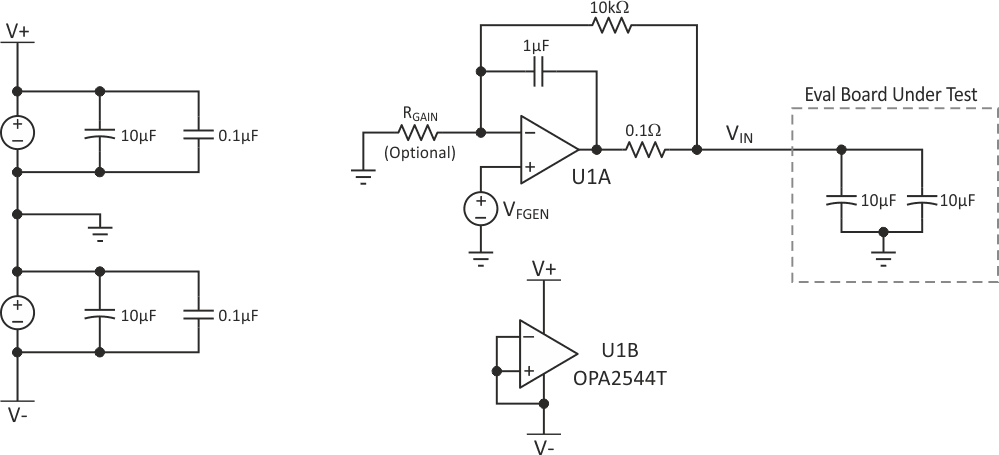
After several failed attempts at rigging up a solution with a function generator in series with a power supply, I came up with the circuit shown in Figure 1. This circuit itself is the product of several revisions of tinkering on the bench to see what worked best. In a nutshell, the desired voltage transient is created on a function generator and buffered using a high power op-amp to drive the 20 µF of capacitance on the evaluation board.
 |
|
| Figure 1. | Line transient tester schematic. |
The heart of this circuit is an OPA2544T from Burr-Brown/Texas Instruments, which is capable of operating from ±35 V supplies and outputting up to 6 A of current if proper precautions are taken. Although this particular application didn’t call for quite so much power, choosing an amplifier that exceeded my immediate needs allowed for a more general test fixture to be built. Once my validation work was completed, this circuit could be used to test many different regulators, battery chargers, and other circuits with a wide range of input capacitance.
The 0.1 Ω resistor between the output of the op-amp and VIN is in place to prevent excessive ringing when recreating fast pulses from the function generator. This resistor is also the output impedance of the circuit over a wide range of frequencies when the load capacitance is rather large, as is the case here [1]. RGAIN can be added to the circuit to allow for voltage transients outside the range of the function generator (±10 V in my case). Putting a minimum resistor in series with a potentiometer for RGAIN is recommended in order to keep the output from saturating should the potentiometer be set incorrectly.
 |
|
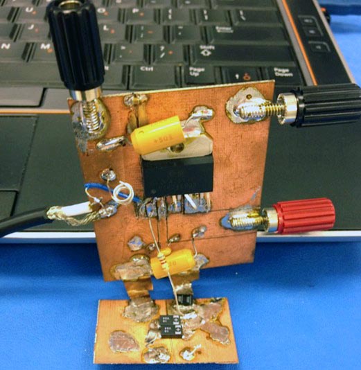
| Figure 2. | Prototyped circuit. |
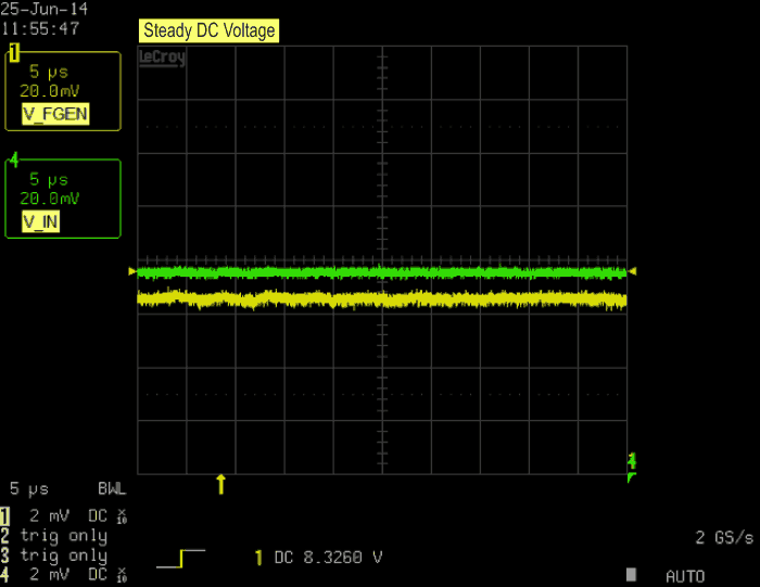
Figure 2 shows the circuit prototyped using copperclad scored with a hobby knife, plus whatever passives I had on hand at my bench. During proof-of-concept testing, a stand-in board was used, with the same 10 µF input capacitors as the real application mounted on a second piece of copperclad. The amount of power drawn by the chip under test was considered negligible and thus ignored at this stage. function generator, as well as between the transient circuit and the input capacitors (note the cut down BNC cable on the left and the copper strips at the bottom). The 0.1 Ω resistance is made from two 0.2 Ω power resistors in parallel to make sure there isn’t any issue carrying high current. While I was feeling out the performance of this circuit I found under certain slew conditions it could become quite warm, so if this ever gets made into a proper circuit board, a heat sink would be a welcome addition. As another general tip, I found the best performance was obtained with at least 6 V of supply headroom on the op-amp relative to the highest or lowest voltage expected (Figure 3).
 |
|
| Figure 3. | Providing a DC voltage. |
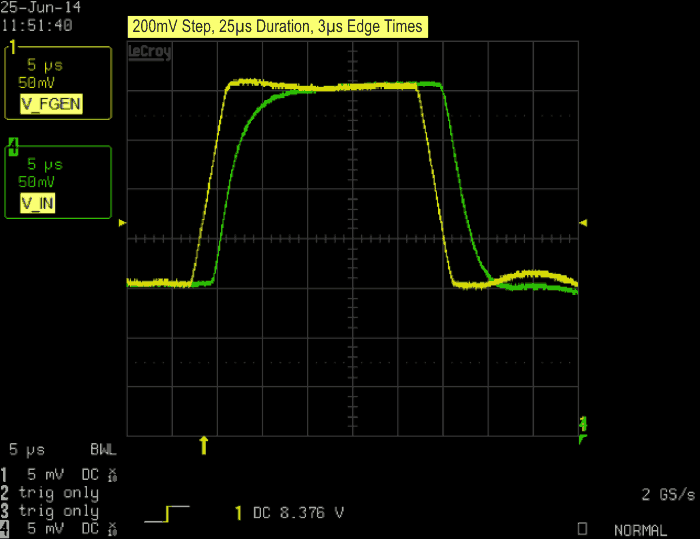
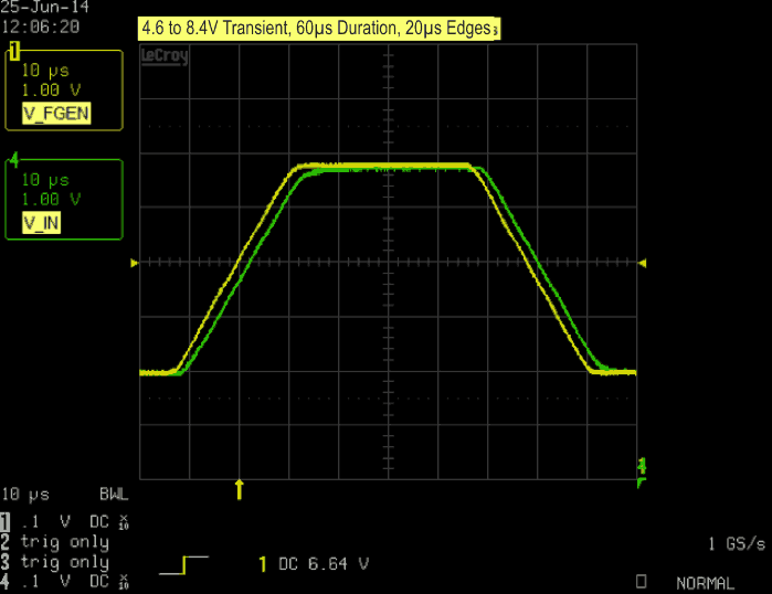
Figures 4 and 5 show the performance of the transient circuit under small, fast line steps and large, slow transients. While not perfect for very fast transients, the prototype performed more than adequately for testing the self-recovery function of the IC. The lack of ringing on either edge meant no false triggers occurred in the chip, I was able to successfully complete the required validation in time to make my deadline, and there was much rejoicing. For recreating larger, slower waveforms from the function generator, the results were even better, showing a stable, though slightly over-damped system.
 |
|
| Figure 4. | Small, fast edge transient results. |
Being able to use a function generator’s many waveform options provides the ability to replicate any line transients expected in the end application, from simple level changes to more complex glitches, in a controlled and repeatable manner. So long as proper precautions are taken to protect the amplifier and board under test, this simple circuit will facilitate more complete validation, and catch any relevant bugs early in the product cycle.
 |
|
| Figure 5. | Large, slow edge transient results. |