The advent of instrumentation amplifiers with digital gain switching offers obvious advantages, such as board-space saving, higher reliability because of fewer solder joints, and lower total cost. These valuable features stem from the fact that the gain-setting networks are integral parts of the monolithic ICs. This feature makes these IC amplifiers much less sensitive to stray electromagnetic fields because the area of internal resistors is a negligible fraction of the previously used discrete gain-setting resistors. Moreover, the value of the relative permittivity of the plastic package and that of the silicon chip are higher than that of the air. As a consequence, the field strength of the electrical component of any stray field penetrating into the chip is lower than that in the surroundings.
Because the gain-setting circuitry is inaccessible directly, a digitally gain-programmable amplifier is a black box. However, the simple fixture in Figure 1 can help to evaluate some of the static characteristics of these ICs. The fixture comprises 10 V REF01 voltage-reference cell, IC1, the elderly but still excellent industry standard, and a high-precision fixed resistive divider. These components provide a millivolt-range output voltage.
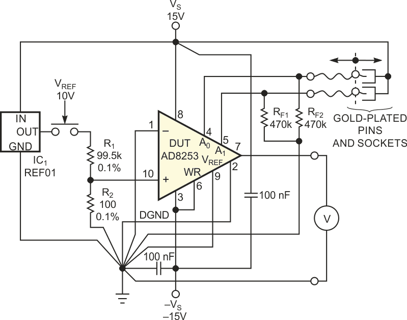 |
|
| Figure 1. | Comprising a handful of components, this circuit allows you to perform your own, independent testing of basic static properties of digitally gain-programmable amplifiers. |
Multiplying the ratio of the resistive divider by the maximum voltage gain of the tested programmable-gain amplifier should give a value of one. The circuit uses tablet-type film resistors having tolerances of 0.1% maximum, yielding a voltage of 10.02 mV at the output of the divider. The two gain-setting logic inputs of the DUT (device under test), an AD8253, connect to short-stranded conductors, which gold-plated pins terminate. Resistors RF1 and RF2 force the logic level at gain-programming inputs A0 and A1 to be low when you disconnect these pins. To set a high level on either or both pins, insert them into the gold-plated counterparts. Two such counterparts interconnect mechanically and electrically and remain at the VS potential. The DUT uses all permutations of the binary values at A0 and A1 logic (see datasheet). The corresponding voltage gains are one, 10, 100, and 1000.
The evaluation procedure involves measuring the output voltage of the DUT with resistor R1 both connecting to and disconnecting from the output of IC1. Thus, you obtain an output voltage of the gain times 10.02 mV and 0 V for all voltage gains. The 0 V output voltage has a nonzero value because of the input-voltage offset; this voltage might seem high at first glance. However, any fraction of a millivolt of the input-voltage offset times a gain of 1000 yields a fraction of a volt at the output.
When you calculate the differences of the 10.02-mV and 0 V output voltages for the respective values of gain, you get a pleasant surprise: These values differ from the ideal values of 10.02 mV times the gain by less than 0.05%. Using this test, you can confirm the precision of the laser-trimmed gain settings. The relatively low value of R2 ensures that the additional input-offset error arising from input bias current of the DUT has a value of less than 3 µV, whereas the typical value is 0.5 µV. Because proper grounding is an absolute necessity when dealing with tens-of-millivolts scale and high-voltage gains, you must connect supply grounds, digital ground, and other rough grounds with the fine signal grounds in one common junction. Figure 1 illustrates this approach by using unusual slanted lines for grounding leads.