| Before proceeding any further, the reader is warned that caution must be used in the construction, testing and use of this circuit. High voltage, lethal potentials are present in this circuit. Extreme caution must be used in working with, and making connections to, this circuit. Repeat: this circuit contains dangerous, high voltage potentials. Use caution. |
 |
|
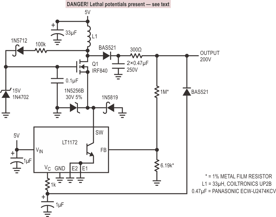
| Figure 1. | 5 V to 200 V output converter for APD bias. Cascoded Q1 switches high voltage, allowing low voltage regulator to control output. Diode clamps protect regulator from transient events; 100k path bootstraps Q1’s gate drive from L1’s flyback events. Output connected 300Ω-diode combination provides short-circuit protection. |
Avalanche photodiodes (APD) require high voltage bias. Figure 1’s design provides 200 V from a 5 V input. The circuit is a basic inductor flyback boost regulator with a major important deviation. Q1, a high voltage device, has been interposed between the LT1172 switching regulator and the inductor. This permits the regulator to control Q1’s high voltage switching without undergoing high voltage stress. Q1, operating as a «cascode» with the LT1172’s internal switch, withstands L1’s high voltage flyback events. Diodes associated with Q1’s source terminal clamp L1 originated spikes arriving via Q1’s junction capacitance. The high voltage is rectified and filtered, forming the circuit’s output. C at the VC pin provides frequency compensation. The 100k path from L1 bootstraps Q1’s gate drive to about 10 V, ensuring saturation. The output connected 300Ω-diode combination provides short-circuit protection by shutting down the LT1172 if the output is accidentally grounded.
 |
|
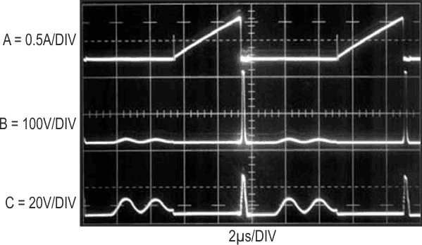
| Figure 2. | Waveforms for 5 V to 200 V converter include LT1172 switch current and voltage (traces A and C, respectively) and Q1’s drain voltage (trace B). Current ramp termination results in high voltage flyback event at Q1 drain. Safely attenuated version appears at LT1172 switch. Sinosoidal signature, due to inductor ring-off between current conduction cycles, is harmless. All traces intensified near center screen for photographic clarity. |
Figure 2 shows operating waveforms. Traces A and C are LT1172 switch current and voltage, respectively. Q1’s drain is trace B. Current ramp termination results in a high voltage flyback event at Q1’s drain. A safely attenuated version of the flyback appears at the LT1172 switch. The sinosoidal signature, due to inductor ring-off between conduction cycles, is harmless.