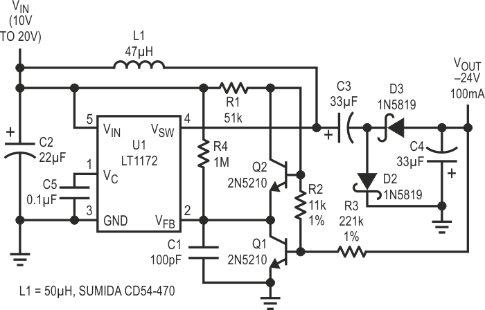
Various switching regulator circuits exist to provide positive- to-negative conversion. Unfortunately, most controllers cannot sense the negative output directly; they require a positive feedback signal derived from the negative output. This creates a problem. The circuit presented in Figure 1 provides an easy solution.
 |
|
| Figure 1. | 10V/20V to –24 converter. |
The LT1172 is a versatile switching regulator that contains an onboard 100 kHz PWM controller and a power switching transistor. Figure 1 shows the LTC1172 configured to provide a negative output using a popular charge pump technique. When the switch turns on, current builds up in the inductor. At the same time the charge on C3 is transferred to output capacitor C4. During the switch off-time, energy stored in the inductor charges capacitor C3. A special DC level-shifting feedback circuit consisting of Q1, Q2, and R1 to R4 senses the negative output.
Under normal conditions Q1’s base is biased at a level about 0.6 V above ground and the current through resistor R3 is set by the output voltage. If we assume that the base current is negligible, then R3’s current also flows through R2, biasing Q2’s collector at a positive voltage proportional to the negative output.
Q2 is connected as a diode and is used to compensate for Q1’s base-emitter voltage change with temperature and collector current. Both transistors see the same collector current and their base-emitter voltages track quite well. Because the base-emitter voltages cancel, the voltage across R2 also appears on the LT1172’s feedback pin, VFB.
The resulting output voltage is given by the following formula:
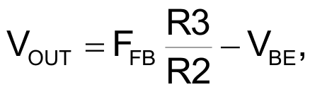
where VFB is the LT1172 internal 1.244 V reference and VBE is Q1’s base/emitter voltage (≈0.6 V). The VBE term in the equation denotes a minor output voltage dependency on input voltage and temperature. However, the variation due to this factor is usually well below 1%.
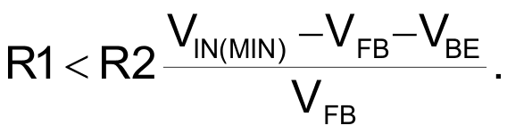
Essentially, Q1 holds its collector voltage constant by changing its collector current and will function properly as long as some collector current exists. This puts the following limitation on R1: at minimum input voltage the current through R1 must exceed the current through R2. This is reflected by the following inequality:
If the input voltage drops below the specified limit (e.g., under a slow start-up condition) and Q1 turns off, R4 provides the LT1172 Feedback pin with a positive bias and the output voltage decreases. Without R4 the Feedback pin would not get an adequate positive signal, forcing the LT1172 to provide excessive output voltage and resulting in possible circuit damage.
The feedback configuration described above is simple yet very versatile. Only resistor value changes are required for the circuit to accommodate a variety of input and output voltages. Exactly the same feedback technique can be used with flyback, “Cuk” or inverting topologies, or whenever it is necessary to sense a negative output.