Low-cost monolithic precision adjustable voltage references are available in multiple families from multiple manufacturers, but this isn’t true for adjustable precision current references. That’s unfortunate, because while most precision analog applications can be made to work with either and a current reference would often be the better fit.
The current reference idea presented here is a simple design for both a current source and current sink that offers good versatility and performance at a budget price. The write-up will conclude with an example of an application that really needed a good current source. Here’s how it works.
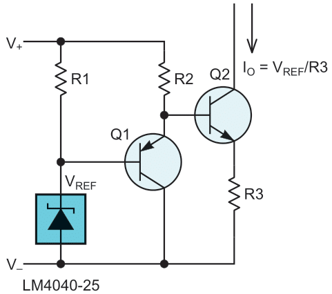
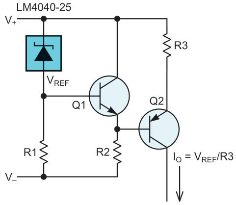
Figure 1 shows the current sink configuration.
 |
|
| Figure 1. | Adjustable current sink with good precision and other desirable characteristics. |
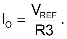
To start with, a 2.5-volt voltage reference is produced by an inexpensive shunt regulator chip. The long-used and widely available (and cheap) LM4040 is illustrated, but many similar performing devices can be used equally successfully, as could other choices (i.e., higher, or lower) for VREF. R1 should be chosen to satisfy the manufacturer’s specified optimum bias current (IREF) for the reference.
For the LM4040, this is ~1 mA. Q1 then buffers, offsets, and temperature compensates VREF for input to Q2. This temperature compensation works best if the collector currents of Q1 and Q2 are made equal, which will result in:
The equal-but-opposite ~2 mV/°C tempcos of the two transistors then cancel each other, and result in a temperature independent output current of:
Voltage compliance is good as Q2 saturation and loss of regulation occur only if VOUT drops to within a couple hundred millivolts of V– + VREF. Choose Q1 and Q2 for complementary symmetry and ratings (e.g., VCE limits) that are compatible with the intended application. The 2N3904 and 2N3906 are typically good choices.
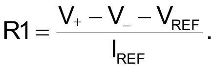
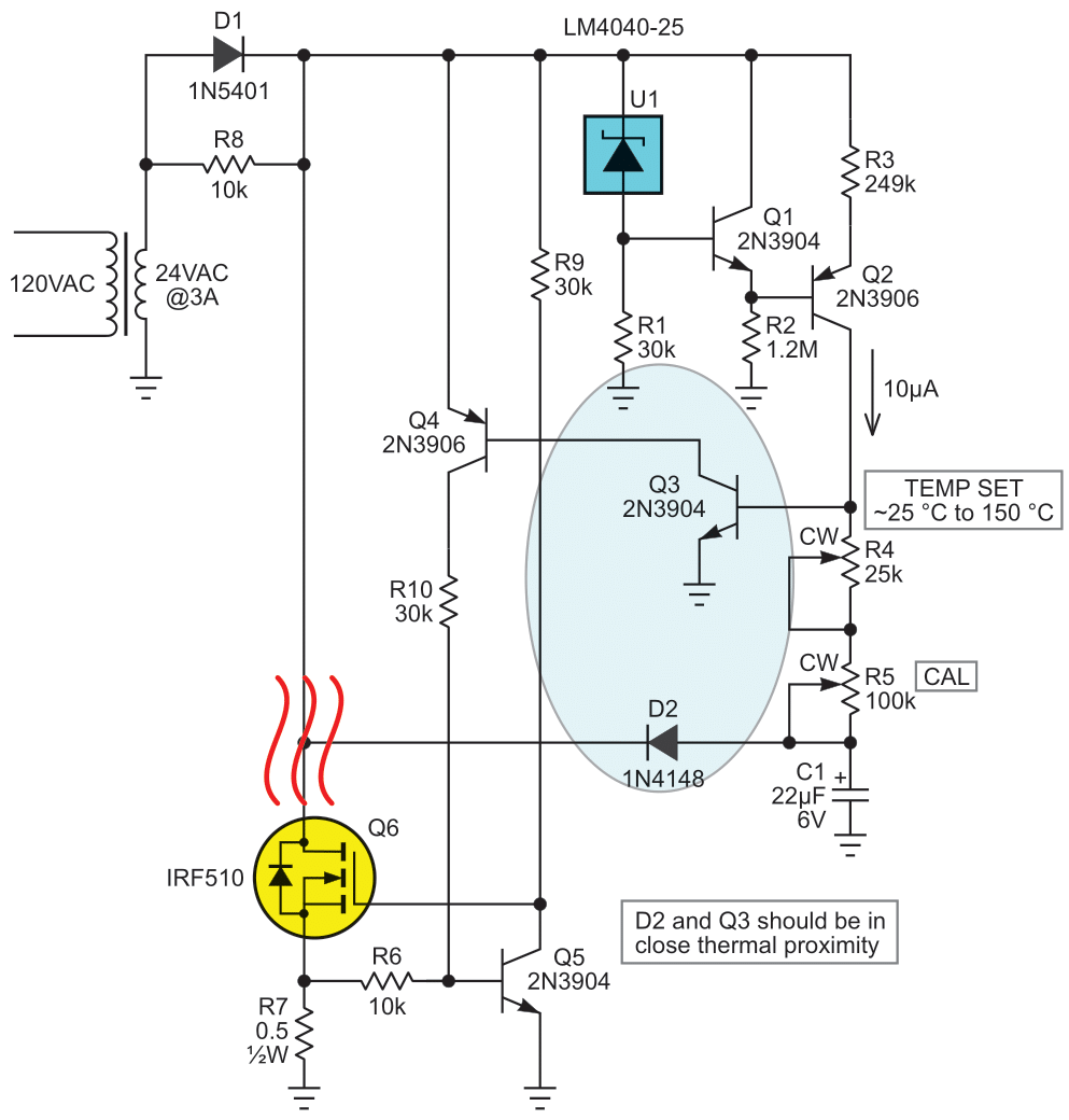
Figure 2 shows the current source version. Its design equations are the same as those of the current sink circuit.
 |
|
| Figure 2. | Adjustable current source with characteristics similar to Figure 1’s sink. |
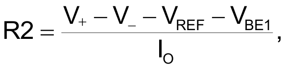
Figure 3 shows an application that derives particular benefit from incorporating Figure 2’s reference. It borrows from an earlier design idea by Ralf Ohmberger (Ref. 1).
 |
|
| Figure 3. | Self-sensing MOSFET thermostat using precision current source for temperature setpoint reference. |
MOSFET Q6 is employed as a combination temperature sensor and heater, the former function is provided by Q6’s FET “parasitic” body diode with current through R8 during the negative AC half-cycle. The latter function relies on normal FET forward conduction of current provided through D1 during the positive AC half-cycle.
Thermostat circuitry closes a feedback loop so that the negative-half-cycle body diode voltage sampled by D2 is compared to the R4 TEMP SET temperature control setpoint and the difference is used to control transistor heating via the Q3, Q4, Q5 signal path. Maximum Q6 heating power is 24 VAC × 1.5 A/2 = 18 W, which is utilized for Q6 heating with an efficiency of ~93%.
Although the integrated MOSFET body diode characterized in the earlier referenced design idea had a tempco of only –0.807 mV/°C, the IRF510 MOSFET (Q6) datasheet (Refer to Figure 7 of its datasheet) shows a larger (and more diode-typical) –2 mV/°C tempco. Because the temperature sense voltage is sampled by D2 and stored on hold capacitor C1 during the negative AC half-cycle, but doesn’t take effect until the heating interval during the subsequent positive AC half-cycle, it must be held with a droop rate no faster than:
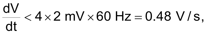
if thermostat stability on the order of single digit °C is to be achieved.
C1 droop is determined by the 10 µA sourced by Q2, therefore C1 = 22 µF results in:
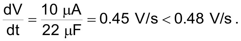
So that works.
If left uncompensated, sampling diode D2’s 2 mV/°C tempco would cause ambient temperature drift to appear one-for-one in Q6 junction temperature. This would contradict the basic definition of thermostasis: that the controlled temperature be (at least mostly) independent of ambient. Fortunately, Q3 has a matching but opposing 2 mV/°C tempco which, when cascaded with D2, results in good cancellation of net drift.
But this scheme only works because the temperature setpoint reference is current, rather than voltage. This matters because, if a reference voltage instead of current were used, adjustment of the setpoint would introduce variable attenuation of Q3’s tempco, which would spoil accurate cancellation of D2’s tempco by Q3’s. The very large (many megaohms) impedance of Q2’s current source avoids this effect, and is one reason a current reference is the superior choice for this application.
The basis of Figure 3’s temperature setpoint is the voltage differential created between C1 and Q3 by R4 + R5 interacting with the 10 µA sourced by the U1, Q1, Q2 current reference. This works well if the voltage acquired by D2 and held by C1 – which is ultimately a function of Q6’s junction temperature – is an accurate readout of the temperature of the thermal load attached to Q6, which depends on a solid thermal contact of load and Q6. Accuracy also depends on proper calibration of R4 via adjustment of R5.
Here’s the recommended method.
Thermostat calibration procedure:
- Remove power from thermostat.
- Place Q6 into a temperature stable environment (e.g., at ~25 °C) and allow it to equilibrate.
- Turn R4 and R5 fully counterclockwise.
- Apply power to thermostat.
- While monitoring voltage present at Q6 source pin (junction of R6 and R7), slowly turn R5 clockwise.
- When a signal appears at Q6 source, stop immediately.
Calibration is now complete.
R4 will now be calibrated for a temperature setpoint range of ~25 °C (fully counterclockwise) to 150 °C (fully clockwise). Note that, as a fail-safe feature, if any or all of the connections to either R4 or R5 (or both) should fail and lose contact, the thermostat will either continue to operate normally or else safely immediately turn off and remove all heating from Q6. This is another free benefit from using a current instead of voltage reference.
Another circuit feature worth mentioning is the de-rating applied to the 24 VAC power transformer. Although peak current draw is limited by Q5 to less than 1.5 A, the transformer is rated for twice that: 3 A. This factor-of-two derating is prudent because of the half-wave conduction of Q6 that’s restricted to the positive AC half-cycle. Half-wave conduction characteristically introduces a strong DC component into the transformer secondary. This can result in core saturation and overheating.
Reference
- Ralf Ohmberger, “Measure junction temperature using the MOSFET body diode”.