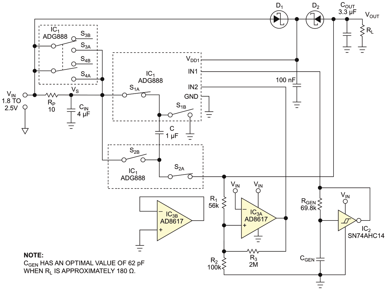
The voltage-doubler circuit in Figure 1 can convert 2.5 V dc to 5 V dc or 1.8 V to 3.3 V. Most voltage doublers use an inductor, but this circuit doesn’t need one. The circuit uses a capacitor, C, by charging it through serially connected switches. The charge switches let capacitor C charge, and the discharge switches are open. In the subsequent discharging phase, the charge switches are off, and the discharge switches close. The two discharge switches now connect capacitor C between the source of the input voltage, VS, and the output capacitor, COUT. This connection scheme lets the applied voltages combine. Thus, the voltage at the output terminal has a value close to 2VS.
 |
|
| Figure 1. | You can use this step-up dc/dc converter in applications in which power efficiency is a critical issue. |
The two phases of operation repeat periodically at frequency f, which clock generator IC2 determines. The duty cycle is about 50%, but the value isn’t all that critical. One half of the Analog Devices high-performance ADG888 analog multi-switch provides the switching. The IC’s two halves have independent control, so the other half occasionally shorts RP, the 10 Ω inrush-current-limiting resistor, which protects the charge switches from an initial overcurrent. That current occurs after power-on, before the output voltage reaches the predetermined percentage of the output’s full voltage.
A micropower op amp, IC3A, runs as a comparator with hysteresis. It compares input voltage to output voltage. Its output starts low and then goes high, which turns on paralleled switches S3 and S4. The comparator’s action is ratiometric because the reference input voltage at the inverting input is the input-supply voltage, VIN. This connection is possible because of the AD8617’s rail-to-rail input/output operation. The circuit also provides overload protection for an excessive load, which connects to the circuit’s output before power-on.
During soft start, the output voltage can’t reach the threshold level for loads below a certain value. Consequently, the circuit remains in soft-start mode. The minimum value of RL, which activates the protective subcircuit, is

where the multiplication factor m = (VOUT/VIN) and α is a fraction of VOUT, at which the soft start turns off. For m = 2, α = 0.8, and RP = 10 Ω, RL is 160 Ω. Thus, loads of 160 Ω or less will overload the circuit if you connect them to the circuit’s output before power-on. IC2 and IC3 get their power from the input supply. IC1, however, switches voltages of as much as 2VIN, and its VDD1 supply-voltage pin must remain at the same level. An analog OR switch comprising Schottky barrier diodes D1 and D2 provides that voltage. The higher of the input or output voltages appears at the VDD1 pin of IC1. The high levels of output voltages for both IC2 and IC3 suffice for control of IC1 because the ADG888’s data sheet allows a 0.36VDD1 value for the high value at the control inputs.
The circuit has been tested at an input voltage of 2.386 V, RL of 178.46 Ω, a frequency of 200 kHz, a supply voltage of 2.377 V, an input supply current of 51.285 mA, and an output voltage of 4.588 V. Evaluating these data gives a multiplication factor of 1.929 and power efficiency of 96.39%.
This power efficiency remains more than 96% for frequencies of 150 to 350 kHz. The 9-mV drop at the switch-shorted RP at the given input current indicates that the on-resistance of the paralleled switches has a value of approximately 0.175 Ω.