Some industrial applications require you to feed a low-power dc/dc converter from a three-phase source and possibly to deal with line-to-line voltages of 200 or 400 V rms. Further, the neutral terminal of the ac source may be unavailable for connection, forcing you to use a line-to-line voltage link, which means a higher input voltage. Voltage faults can happen in one or two phases, and some applications require the power supply to keep working despite this problem. To handle these problems, you can use an uncontrolled rectifier and a capacitor to convert three-phase ac into a dc voltage, but this voltage may be higher than the maximum input voltage that a standard converter supports. It is difficult to find a dc/dc converter for these voltages, which are typically 564 V dc or higher.
 |
|
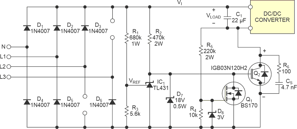
| Figure 1. | A three-phase rectifier uses a switched IGBT and a capacitor to reduce the voltage to standard offline dc/dc converters. |
You can use the circuit in Figure 1 to obtain a dc voltage lower than a given value, which the ratio of R1 to R3 sets. This value is approximately 340 V peak with the values in the figure, from a 400 V-rms or higher line-to-line three-phase voltage. You can feed this value from two or three phases with or without the neutral wire or from just one phase with the neutral wire. This circuit omits two diodes from the typical three-phase rectifier bridge and includes a neutral wire diode pair to obtain voltages below 340 V across bulk capacitor C1 and to reach 0 V for initial start-up (Figure 2). If you connect the neutral wire, you must link it to a two-diode arm of the rectifier to achieve a 0 V start-up; however, you can randomly connect the phase wires.
 |
|
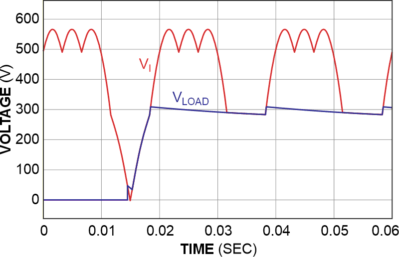
| Figure 2. | This circuit omits two diodes from the typical three-phase rectifier bridge and includes a neutral-wire diode pair to obtain voltages below 340 V across bulk capacitor C1 and to reach 0 V for initial start-up. |
Shunt regulator IC1 acts as a comparator. After the initial start-up, whenever the instantaneous rectified voltage, VI, is higher than 340 V, the IC1 reference-to-anode voltage is higher than its internal reference of 2.495 V, decreasing the anode-to-cathode voltage to approximately 2 V and turning off Q2. When rectified voltage is lower than 340 V, IC1 does not sink current. Thus, Q2 turns on through the R2 bias, connecting bulk capacitor C1 and the dc/dc-converter load to the rectifier.
At turn-on, if C1 is completely discharged and the instantaneous rectified ac-line voltage is greater than approximately 50 V, MOSFET Q1 is on, keeping insulated-gate bipolar transistor Q2 off; no charging current flows into the capacitor. If the instantaneous rectified voltage is lower than the voltage across the bulk capacitor plus 50 V, Q1 is off and Q2 turns on, connecting the capacitor and the load to the rectifier.
Notice that, especially at turn-on, the value of Q2’s VCE = VI – VLOAD rises to large values when Q2 turns off, so R5 must be as large as possible and must handle approximately 0.5 W of power. Increasing the value of R5 means that you must increase the value of R4, more slowly turning off Q1 and possibly resulting in a start-up malfunction. You must reach a practical compromise for the values of R4, R5, and D8. Considering that D8 limits the maximum gate voltage at Q1, it must have a zener voltage as close as possible to the threshold voltage for a faster turn-off through R4. A BS170 is a good choice for Q1. You can add a snubber network comprising R6 and CS across the collector-emitter of Q2 to limit the generated noise.
With the actual load voltage at 340 V, IC1’s reference voltage is approximately 0.5 V higher than its cathode, and the input transistor begins to conduct through the base-collector junction. You must measure this cathode voltage at 45 μA at 0.5 V, and you must account for this value if calculating new values for R1 and R3. The simulation in Figure 2 does not account for this input leakage and appears to switch at 310 V.