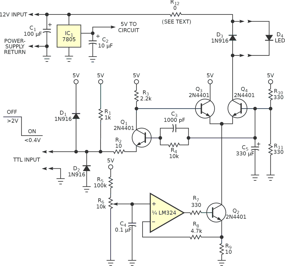
Applications such as turbidity measurement and densitometry require cleanly pulsed light sources with stable amplitudes. The LED driver in Figure 1 illuminates retinal neurons in a biological experiment that has similar requirements. For a given LED at a given current, the intensity is stable, so switching a stable current is a simple and effective way to obtain the needed function. The circuit provides current pulses to the LED with rise and fall times lower than 500 nsec and overshoot lower than 7%. You can make the current computer-programmable by replacing the potentiometer with a DAC. The circuit comprises an adjustable, regulated current source (IC1 and Q2 ), an overdriven differential amplifier (Q3 and Q4 ) acting as a switch, and a level shifter (Q1 ) to shift the TTL input signal to levels needed to drive the differential pair.
 |
|
| Figure 1. | This circuit delivers a stable, precision dose of current to an LED. |
Voltage at the wiper of R6 results in an equal voltage across R9 because of feedback to the op amp. Because transistor Q2 has a high alpha, most of the emitter current that produces the voltage across R9 comes from the collector of Q2. Because alpha varies little with temperature, this current remains stable. Transistors Q3 and Q4 constitute a differential pair. Depending on which transistor is conducting, the emitter of one or the other sources current to the collector of Q2. When the base of Q3 becomes several hundred millivolts more positive than the base of Q4, current from Q2 shunts to the 5 V power supply. No current flows through, so the LED is off. When the base of Q3 is less positive than that of Q4, current from Q2 passes through the LED. The all-or-nothing switching action results from the large differential voltage across the bases. Similar to the case of Q2, the collector current in Q4, when it is conducting, is a high and stable percentage of the emitter current. The constant load the emitters of Q3 and Q4 present to the current source enables the current source to operate continuously, allowing the use of a low-bandwidth op amp.
Q1 is a common-base amplifier connected in a manner essentially the same as a TTL-input stage with the exception of C3, the 1000-pF capacitor across base resistor R4. When the input signal is greater than 2 V, the base of Q1 remains at 2.5 V, and the collector of Q1 rises enough to ensure that Q4 and the LED conduct no current. When the input is below 0.4 V, Q1’s emitter voltage is low enough and the base current through R4 is high enough to saturate Q1. This action holds the base of Q3 low enough to ensure that all the collector current from Q2 passes through Q4 and the LED. When the input signal swings positive again, the energy stored in C3 develops a reverse bias across Q1’s emitter-base junction to quickly deplete the stored charge, resulting in a rapid turn-off. Make sure that you don't exceed the power rating of Q4. Take the current and collector-to-emitter voltage into account. Using transistors in TO-92 packages and an LED that drops 2 V at 50 mA, the circuit in Figure 1 operates at temperatures greater than 55 °C with a jumper in place of R12. If you need higher currents or use smaller transistor packages, you may find it necessary to use a finite resistor for R12 to lower the dissipation in Q4 to a safe level.