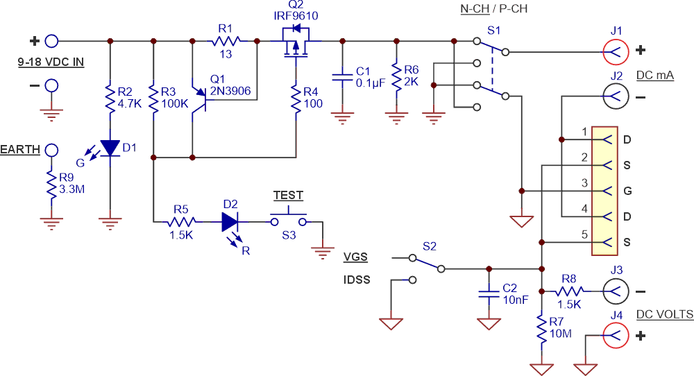
The circuit presented by Cor van Rij (Ref. 1) for characterizing JFETs is a clever solution. Noteworthy is the use of a five-pin test socket wired to accommodate all of the possible JFET pinout arrangements.
This idea uses that socket arrangement in a simpler circuit. The only requirement is the availability of two digital multimeters (DMMs), which add the benefit of having a hold function to the measurements. In addition to accuracy, the other goals in developing this tester were:
- It must be simple enough to allow construction without a custom printed circuit board, as only one tester was required.
- Use components on hand as much as possible.
- Accommodate both N- and P-channel devices while using a single voltage supply.
- Use a wide range of supply voltages.
- Incorporate a current limit with LED indication when the limit is reached.
The circuit
The resulting circuit is shown in Figure 1.
 |
|
| Figure 1. | Characterizing JFETs using a socket arrangement. The fixture requires the use of two DMMs. |
Q1, Q2, R1, R3, R5, D2, and TEST pushbutton S3 comprise the simple current limit circuit (R4 is a parasitic Q-killer).
S3 supplies power to S1, the polarity reversal switch, and S2 selects the measurement. J1 and J2 are banana jacks for the DMM set to read the drain current. J3 and J4 are banana jacks for the DMM set to read VGS(OFF).
Note the polarities of the DMM jacks. They are arranged so that the drain current and VGS(OFF) read correctly for the type of JFET being tested – positive IDSS and negative VGS(OFF) for N-channel devices and negative IDSS and positive VGS(OFF) for P-channel devices.
R2 and D1 indicate the incoming power, while R6 provides a minimum load for the current limiter. Resistor R8 isolates the DUT from the effects of DMM-lead parasitics, and R9 provides a path to earth ground for static dissipation.
Testing JFETs
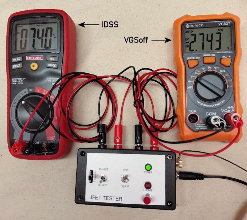
Figure 2 shows the tester setup measuring VGS(OFF) and IDSS for an MPF102, an N-channel device. The specified values of this device are VGS(OFF) of –8 V maximum and IDSS of 2 to 20 mA. Note that the hold function of the meters was used to maintain the measurements for the photograph. The supply for this implementation is a nominal 12-volt “wall wart” salvaged from a defunct router.
 |
|
| Figure 2. | The test of an MPF4392 N-Channel JFET using the JFET characterization circuit. |
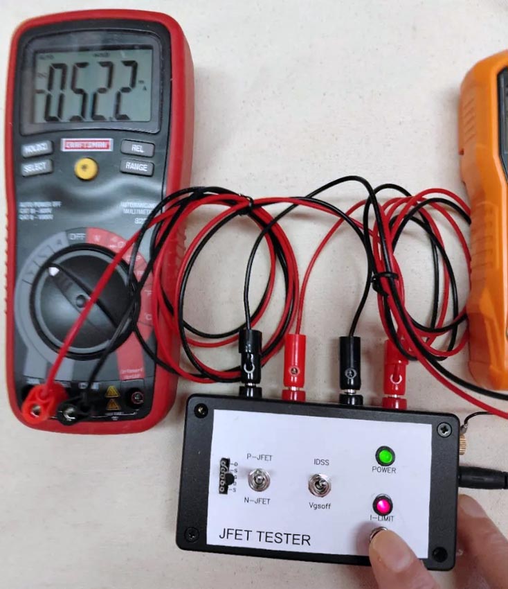
Figure 3 shows the current limit in action by setting the N-JFET/P-JFET switch to P-JFET for the N-channel MPF102. The limit is 52.2 mA, and the I-LIMIT LED is brightly lit.
 |
|
| Figure 3. | The current limit test that sets the N-JFET/P-JFET switch to P-JFET for the N-channel MPF102. |