In April 2012, EDN published a circuit by John Fattaruso (Ref. 1) that lets you quickly measure the drain-source saturation current and the pinch-off voltage of both an N-JFET and a P-JFET. The pinch-off voltage (VP) is measured by inserting a very large resistance between the source and the ground. The drain-source saturation current (IDSS) is measured by inserting a small resistance between the source and the ground. Then, the voltage across this resistor is measured, and both VP and IDSS can be calculated using Ohm’s law.
There is a catch with this circuit: Since IDSS is measured across a non-zero resistor, there is a deviation from the real IDSS, see Figure 1. This circuit does not really measure point A, but actually measures point B slightly before this. For JFETs with lower VP voltages and/or higher IDSS currents, there can be a deviation between the measured and real IDSS value of 5% or more.
 |
|
| Figure 1. | A standard N-JFET drain-source current vs gate-source voltage curve. |
Circuit idea
The accuracy of the circuit can be drastically increased by making a couple of minor changes. Figure 2 shows the basic circuit.
 |
|
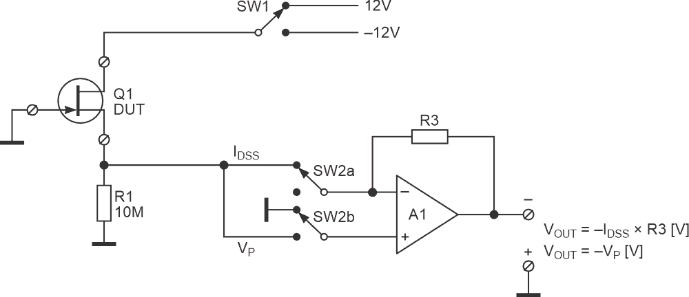
| Figure 2. | A basic, improved circuit for the JFET IDSS and VP measurement. |
An astute reader will immediately see the two circuits’ similarities and differences. Switch 1 is, again, used to select between N-channel JFETs and their less common sibling: P-channel JFETs.
Switch 2 is used to select between VP and IDSS measurement. In the position as drawn, IDSS is measured. In this position, A1 is set up as a transimpedance amplifier.
With the op-amp’s non-inverting input connected to ground, A1 will keep the inverting input, and hence the source, to ground as well. This guarantees that the true IDSS is measured. Resistor R3 then converts the current to a voltage that can be measured at the output of A1.
When Switch 2 is flipped to the other position, A1 is set up as a simple voltage follower. The pinch-off voltage that develops across R1 is then buffered and available at the output of A1.
Full implementation
Now that we have seen the basic circuit, we can look at a full implementation (Figure 3). Resistor R2 limits the current that can flow in case a JFET is inserted incorrectly. In pinch-off measurement mode, the impedances around Q1, R1 and A1 are all pretty high. To limit the influence of noise, capacitor C1 is added. It is best to keep these wires short and/or to build the circuit in a shielded box.
 |
|
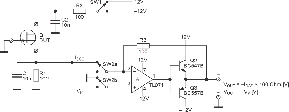
| Figure 3. | First implementation of the practical circuit used to measure IDSS and VP. |
Most operational amplifiers can only source or sink a small amount of current. The drain-source saturation current can easily be in the tens of milliamperes. To boost the current output capabilities of A1, a complementary bipolar transistor output stage is added. Please note that the output is not short-circuit proof. If preferred, a simple 1 kΩ to 10 kΩ resistor can be added in series with the output.
With the current resistor values in the circuit, a pinch-off voltage of ±10 V can be measured and a saturation current of ~ ±100 mA.
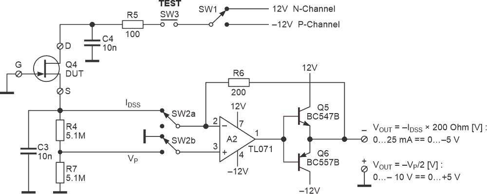
Although there are JFETs with large saturation currents (think J109 with IDSS > 40 mA and J108 with IDSS > 80 mA!), this is simply not needed for most JFETs. So, a variation on this circuit was developed. The pinch-off voltage remained the same, but the saturation current was returned to 25 mA, covering almost all JFET types. A further requirement was that the output voltage range for both measurements needed to be the same: 0 … ±5 V. This was so that a moving coil meter readout could be used with a single range.
See Figure 4 for the implementation.
 |
|
| Figure 4. | A circuit with the tailored measurement range that is suited for most JFETs. |
Read-out
A read-out needs to be added to make this a complete measurement instrument. Since I have a large stock of moving coil meters, I decided to use one of these for the read-out. To some, they may look antiquated, but they are a joy to use and a marvel of mechanical engineering! The output can be positive or negative depending on whether you are measuring VP or IDSS, and whether an N-type JFET or a P-type JFET is being tested. So, this is something that needs to be dealt with. Also, it would be nice if there were some kind of polarity indication. See Figure 5 for the read-out circuit.
 |
|
| Figure 5. | The readout circuit with sensitive polarity indication. |
The 1-mA moving coil meter is included in the feedback loop around the op-amp. D3-D6 form a common rectifier bridge so that, independent of the polarity of the input voltage, the meter is always fed a positive current.
Transistors Q1 and Q2 serve as a polarity indication. Positive voltages will turn on Q1 and LED D9. LED D10 will indicate negative voltages.
D7,8 are not needed for the rectification. Because of these diodes, the A1 output voltage must be above/below ±1.8 V before any significant current will flow through the meter. This, in turn, guarantees that transistors Q1 and Q2 will already turn on at very low input voltages, giving a good polarity indication across the whole input range.
Test socket
Over the years, manufacturers have created JFETs with almost every possible pin-out, so making a single universal test socket is not so trivial. With three leads, there are 3! = 6 possible combinations as shown in Table 1.
| Table 1. | The six possible pin-out combinations that can be used for an off-the-shelf JFET |
||||||||||||||||||||||||||||
|
|||||||||||||||||||||||||||||
Of course, a JFET with a pin-out of S-D-G (#6) can be tested in a socket with pin-out G-D-S (#1), simply by inserting it reverse in the socket. This effectively eliminates half of the possible combinations. So we are left with the following three, as shown in Table 2.
| Table 2. | A reduction in the number of pin-out combinations by simply reversing the component within the test socket |
||||||||||||||||||||||||||||
|
|||||||||||||||||||||||||||||
After a bit of doodling, we can create a single five-pin test socket that can accommodate every possible JFET pin-out as shown in Table 3 and in Figure 6.
| Table 3. | A singular 5-pin test socket to accommodate all possible JFET pin-outs |
||||||||||||||
|
|||||||||||||||
 |
|
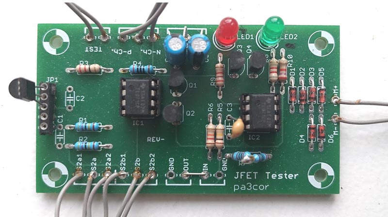
| Figure 6. | The final PCB implementation of the practical JFET circuit used to measure IDSS and VP, showing the test socket. |
There are two different variants possible; this is left as an exercise to the reader. The same logic can be applied to create universal test sockets for bipolar transistors, of course.
In closing
Thanks to John Fattaruso for his excellent design idea, which sprouted this idea! We all stand on the shoulders of the giants that came before us.
Reference
- Fattaruso, John. "Simple circuit lets you characterize JFETs."