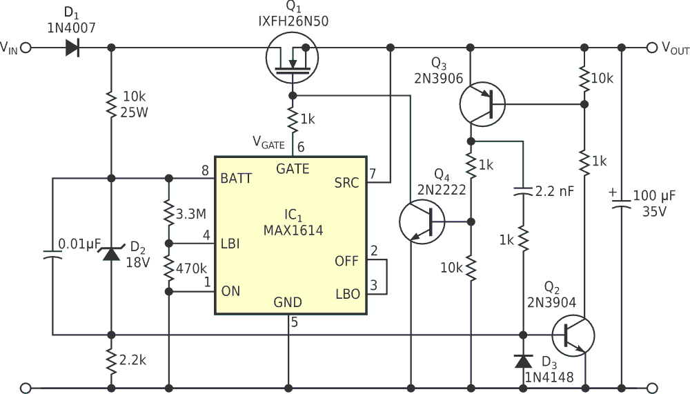
Voltage transients on low-voltage power lines can sometimes attain amplitudes many times the nominal voltage level. That behavior often calls for protection against the application of improper power levels. The usual way to protect sensitive circuitry against overvoltage is to add parallel clamps. Fuses or other current-limiting devices precede these clamps' high energy-absorption capability. Other cases require the use of high-voltage series protection (instead of parallel clamps) because of the difficulty in resetting or replacing fuses, an inaccessible operating environment, or the need for uninterrupted operation. The series-protection circuit of Figure 1 turns off the power switch using a series-connected, high-voltage, n-channel MOSFET power switch, Q1, and a fast overvoltage detector. The power switch and series-connected power rectifier, D1, protect the load against high-voltage transients and continuous overvoltage as high as ±500 V of either polarity.
 |
|
| Figure 1. | This circuit protects a load, connected to the right pair of terminals, from undervoltage and highvoltage transients in the supply voltage, connected to the left pair of terminals. |
In the circuit, which powers loads as heavy as 1 A from a nominal 12 V power line, a high-side-switch driver, IC1, biases the power switch fully on. You can increase the maximum load current by changing D1 and Q1. To guard against low supply voltage, IC1 includes an undervoltage-lockout feature that allows operation only when the line voltage is greater than 10 V. To protect against overvoltage, the circuit includes a three-transistor, no-bias-current, 50-nsec-operation overvoltage detector that triggers when the input voltage reaches approximately 20 V. At that time, Q4 “crowbars” the gate of the power switch to ground, turning it off hard. Rising overvoltage first turns on zener diode D2, which protects the IC by clamping the voltage across it to approximately 18 V. Zener current flows through the 2.2-kΩ resistor, producing a base voltage that turns on Q2. That action initiates a rapid sequence: Q3 turns on, which turns on Q4, which turns off Q1 by quickly discharging its gate capacitance.
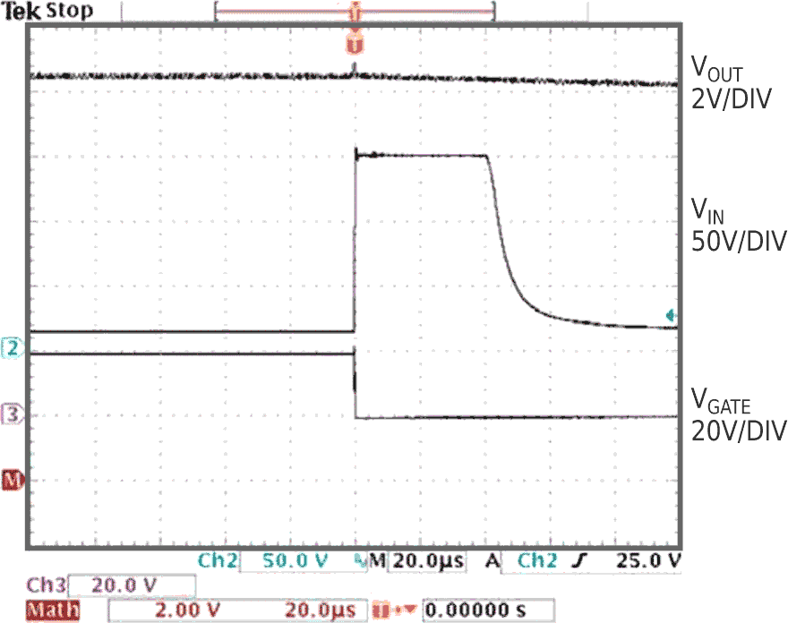
You can demonstrate the circuit's performance by applying a 150 V transient to the supply voltage while the circuit output is delivering 1 A at 12 V (Figure 2). The internal impedance of the transient source is 1 Ω, and the rise time of the applied voltage is 1 µsec. The circuit draws 20 µA during normal operation, including 3 µA by the undervoltage-lockout, voltage-sensing divider and 17 µA by IC1. If your design needs high-temperature operation, note that the gate-current output of IC1 is relatively limited. Your design calculations for high temperature should also pay close attention to leakage currents that the other circuit components contribute.
 |
|
| Figure 2. | A 150 V transient applied to VIN of the Figure 1 circuit has little effect on VOUT. |