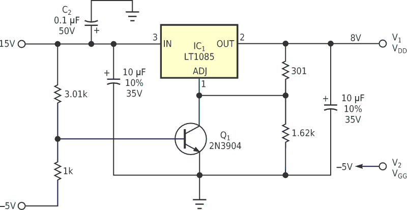
It's important to properly sequence the bias applied to an RF/microwave GaAs FET or a MMIC (monolithic-microwave-IC) amplifier. These devices are extremely sensitive to drain and gate voltage levels as well as to the order in which these biases turn on and off. A GaAs-FET amplifier that uses two bias voltages – a negative supply, VGG, on its gate and a positive supply, VDD, on its drain – requires that VGG be present before the application of VDD. When powering down the amplifier, VDD must go to 0 V before VGG changes from its negative value to 0 V. Figure 1 shows a commonly used disable circuit found in many voltage-regulator data sheets. The circuit uses a 2N3904 switching transistor to pull the ADJ pin to ground to disable the voltage regulator.
 |
|
| Figure 1. | Circuit improves on bias for GaAs FETs. |
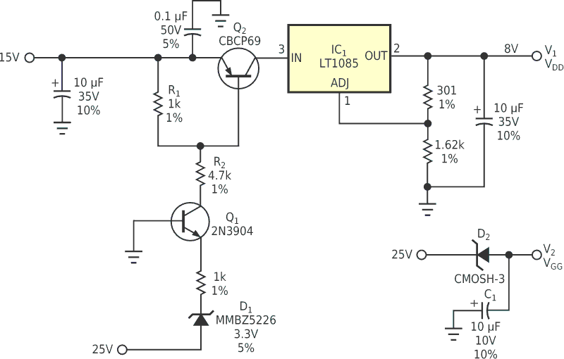
The circuit does not set the output of the regulator to 0 V but instead sets the output to the regulator's reference voltage, 1.25 V. The condition in which a GaAs FET or MMIC has 0 V on the gate and 1.25 on the drain can result in damage to the device. For example, M/A-Com's MAAM26100-PI MMIC power amplifier requires 8 V for VDD and –5 V for VGG. With 1.25 V on VDD and 0 V on VGG, the MMIC draws approximately three times its nominal drain current, sufficient to cause destructive failure. Figure 2 shows an improved circuit for the adjustable regulator.
 |
|
| Figure 2. | This circuit provides safe power-up and power-down sequencing for sensitive GaAs FETs and MMICs. |
A medium-power pass transistor, Q2, a Central Semiconductor CBCP69, connects to the input of the voltage regulator to disable the regulated output voltage. In disabled mode, the voltage at the regulator's output is 0 V. In enabled mode, Q1 saturates and activates a voltage divider comprising R1 and R2. Q2 saturates, and the output swings from 0 to 8 V. Because of the propagation delay of the transistor switching network, the 8 V output switches from 0 to 8 V after the –5 V supply switches from 0 to –5 V. D1 sets the disable threshold of the –5 V supply to approximately –4 V to minimize the delay between the –5 V supply switching from –5 V to 0 V and the regulator switching from 8 V to 0 V. To ensure that VGG remains at –5 V after disabling IC1, you can exploit the high FET gate resistance and the low-leakage Schottky-diode characteristic. The combination of high gate resistance of the GaAs FET, the low-leakage Schottky diode, D2, and the 10-µF capacitor, C1, provides a high VGG RC time constant when the –5 V supply is off (in other words, at 0 V). The RC time constant of the Schottky-diode leakage resistance, the FET gate resistance, and C1 is long compared with the RC time constant at VDD. As well as having low reverse leakage, D2 has an inherently low (0.1 V) forward drop.