Some amplifier applications require clamping or limiting due to large, sporadic signals appearing at the amplifier input. Clamping these errant signals protects the amplifier and other sensitive downstream circuitry. It also improves overdrive recovery time and can lower distortion.
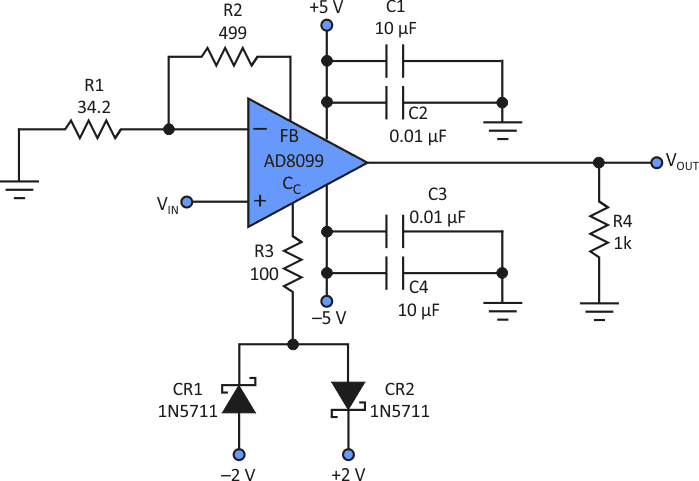
At the heart of the clamp circuit described here is the AD8099 high-speed, low-noise, externally compensated amplifier. The device consists of a single-stage amplifier followed by a unity-gain buffer. External compensation is required in low-gain applications, but not with gains of greater than 10. The clamper exploits that feature by setting the amplifier for a gain of 15, eliminating the need for a compensation network. The compensation pin can then be used in an unconventional manner to provide clamping.
The clamping circuit employs two 1N5711 high-speed Schottky barrier diodes connected to the compensation pin through resistor R3, which limits the current in and out of the compensation pin (Fig. 1). In this application, the current is approximately 6 mA. It should be kept below 10 mA for safe operation.
 |
|
| Figure 1. | This circuit uses the AD8099 amplifier IC in an unconventional way, connecting a clamping network to the amplifier’s compensation pin. |
The diodes perform the lion's share of the clamping function. They feature very low capacitance and picosecond switching, thus maintaining high-frequency performance and crisp transition edges.
The drop across R3 is about 0.6 V, which combines with another 0.4 V across D1 or D2 to make the total drop approximately 1 V. With ±2-V references, the amplifier output clamps at ±3 V.
 |
|
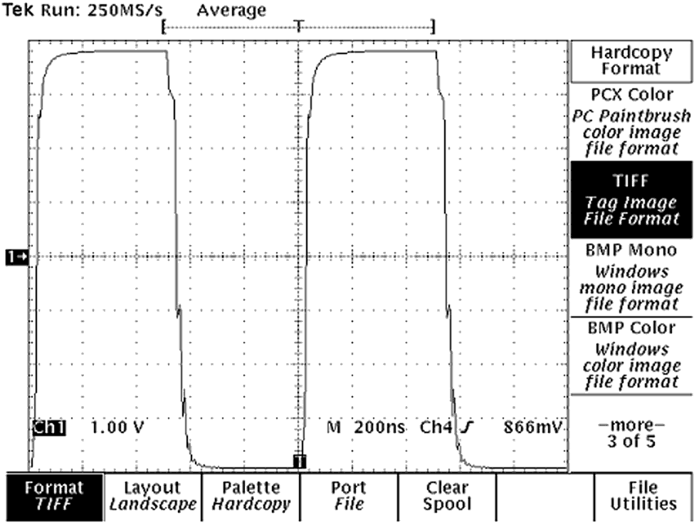
| Figure 2. | Without the clamping network and with the amplifier overdriven, the output clearly shows asymmetry, distortion, and other effects of the overdriving. |
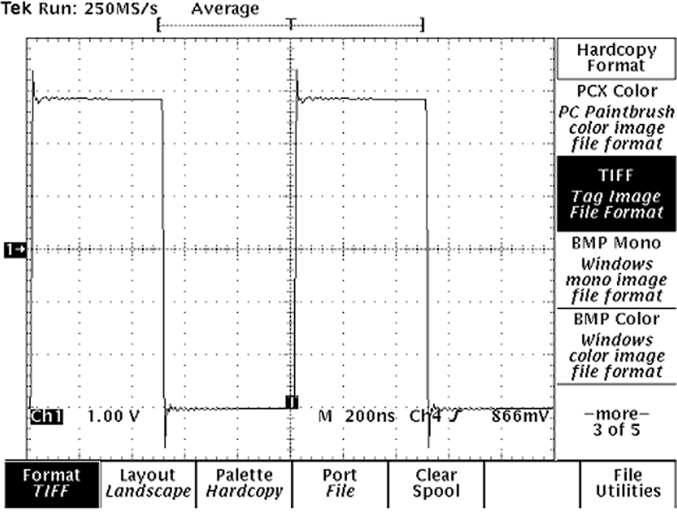
Without the clamping network in place, overdriving the amplifier's input with a 1-V, 5-MHz square wave causes the amplifier to rail. Asymmetry, distortion, and other signs of overdriving are clearly visible at the amplifier's output (Fig. 2). With the clamping circuit incorporated, the output is clamped to ±3 V, and the asymmetry and distortion effects of overdriving have been eliminated (Fig. 3).
 |
|
| Figure 3. | Adding the clamping circuitry eliminates the problems from the amplifier’s output, which are caused by overdriving the input. |