Whenever you hear the transformerless supply term, you initially imagine the capacitor-based solution: a high-voltage non-polarized capacitor in series with the mains line, a bridge rectifier, a Zener diode, and a filtering electrolytic capacitor. Such a circuit does not work efficiently and cannot deliver enough current for many applications. However, you might see such circuits in some low-cost products.
This article uses an advanced Diodes Incorporated AL17150 high-voltage step-down regulator chip that gets universal 85 VAC to 260 VAC at the input and handles 12 V-200 mA at the output. The output voltage can be set to a different level by modifying the feedback resistors. The PCB board is compact, uses SMD components, and can be mounted vertically on the mainboard.
Circuit analysis
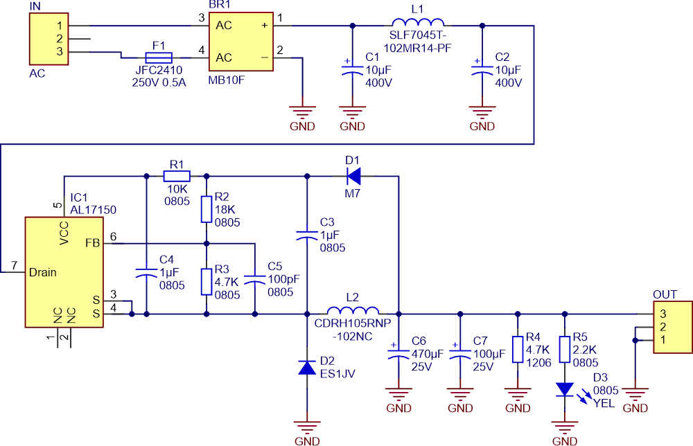
Figure 1 shows the schematic diagram. The heart of the circuit is the AL17150 high-voltage step-down controller chip.
 |
|
| Figure 1. | Schematic diagram transformerless 85-260 VAC to 12 VDC-0.2 A power supply. |
According to the datasheet of the AL17150: “The AL17150-10B is a universal high-voltage input step-down regulator product family, which provides accurate Constant Voltage (CV) and outstanding dynamic performance without requiring an optocoupler over line and load regulation. Typical applications are offline low-power applications including connected LED lighting power supply for microcontrollers and other IoT applications. The AL17150-10B integrates a 500 V/1 A MOSFET that can use fewer external components and create a low Bill of Material (BOM) cost solution. The AL17150-10B can provide up to 300 mA output current and lower than 50 mW standby power, which is very suitable for IoT-connected lighting devices.
The AL17150-10B achieves excellent regulation and high-power efficiency. The characteristics of max peak current and driving frequency vary as the load changes, which can improve efficiency performance at light load and overall average efficiency. The AL17150-10B has rich protection features to enhance the system’s safety and reliability. It has over-temperature Protection, VCC Under Voltage Lock function, Output Short Protection, Over-Load Protection, and Open Loop Protection (220 V AC to 12 V DC converter without transformer). The AL17150-10B is available in the SO-7 package.”
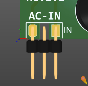
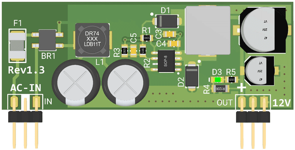
IN is a 3-pin male header, used for the AC input. The PCB board on the middle pin contains a creepage area to follow the high-voltage IPC rules (Figure 2). Similarly, an isolation gap (creepage area) should be created on the mainboard PCB, around the middle pin of the header.
 |
|
| Figure 2. | An isolation gap (creepage area) around the middle pin of the header. |
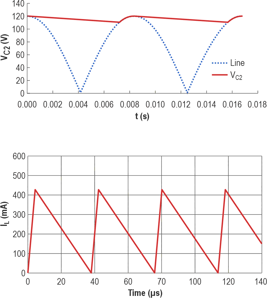
F1 is the JFC2410 250 V-0.5 A fuse for protection. BR1 is the MB10F bridge rectifier, fulfilling the initial stage of AC-to-DC conversion. C1, L1, and C2 build a low-pass Pi filter to reduce the input noise and ripple. IC1 is the AL17150 chip and R2 and R3 are feedback resistors. C5 reduces the high-frequency noises and D2 and L2 build the buck converter circuit. Be careful that D2 is an ultra-fast diode that achieves 35 ns reverse recovery time (Trr). C6 and C7 are output capacitors for noise reduction and output stabilization. R4 is a 1206-4.7K resistor that acts as a dummy load. D3 is a yellow 0805 LED, indicating the output voltage is at a proper level. Figure 3 shows the voltage and current waveforms (simulation) of the C2 capacitor.
 |
|
| Figure 3. | Voltage and current waveforms of C2 (simulation). |
AL17150 buck design tool
The chip man µFacturer (Diodes Incorporated) has introduced an interesting and helpful Microsoft Excel [1] file that can be used for calculation. If you look at the table, there are a few parameters that you could modify to set your desired output voltage and current. The user sets the FB pin low-side resistor and the high-side resistor is calculated by the script. For the 12 V output, the low-side resister is 4.7K and the high-side one is 18K. The output capacitors are two electrolytic-type in parallel to reduce the ESR, so the total output capacitance is 470 µF + 100 µF = 570 µF.
PCB layout
 |
|
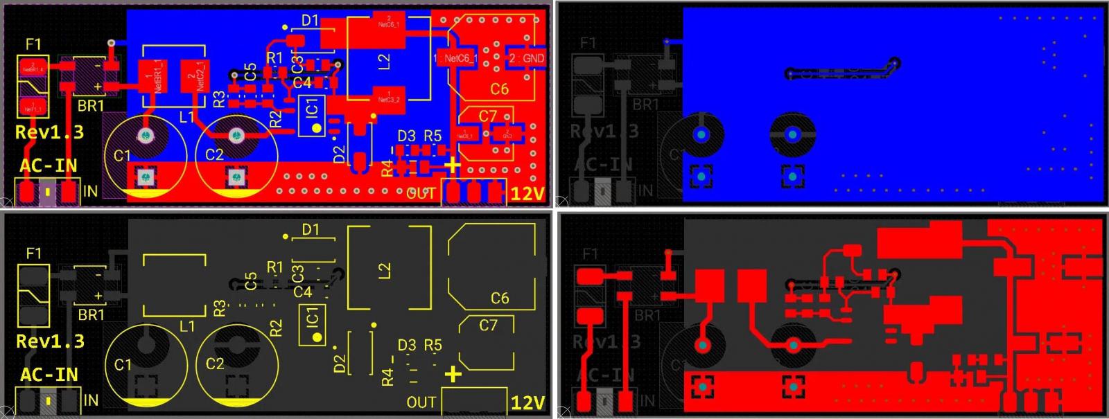
| Figure 4. | PCB layout of the transformerless 85-260 VAC to 12 VDC-0.2 A power supply. |
Figure 4 shows the design’s PCB layout. It’s is a two-layer PCB board with SMD components, the design files for which are available in the Downloads section. The smallest package size is 0805, so you shouldn’t have a problem soldering the components using a normal iron and a good tip, although a micro-soldering station is preferred. Figure 5 shows the assembly drawing.
 |
|
| Figure 5. | Assembly drawing of the PCB board. |
Testing
 |
|
| Figure 6. | An infrared thermal image of the PCB board. |
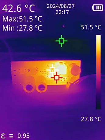
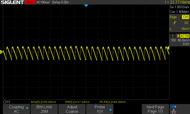
The PCB board has been tested using a DC load, an oscilloscope, and a thermal imaging camera. Figure 6 shows an infrared thermal image of the PCB board after 20 minutes of full operation (200 mA load). The highest temperature was spotted around the controller chip (51 to 52 degrees C) and the room temperature was 28 degrees C. Figure 7 shows the output noise of the power supply, at the maximum output current (around 60 mVp-p). if a lower noise level is expected, you can add one electrolytic (or an electrolytic and a ceramic capacitor in parallel) just next to your load.
 |
|
| Figure 7. | Output noise of the power supply (200 mA load). |
Reference
Downloads
Materials on the topic
- Datasheet Diodes AL17150
- Datasheet Rectron ES1JV
- Datasheet Diotec M7
- Datasheet Diodes MB10F
- Datasheet Sumida CDRH105R
- Datasheet TDK SLF7045