Antonio Munoz
In a prior research project in the communications field, we created a portable, low-frequency (0 to 1 MHz) signal generator design. This generator had a broad output voltage range (0 to 100 Vp-p) and medium current capability (500 mA). It was also rugged and battery powered.
Recently, however, we needed a similar design with one additional capability: arbitrary signal generation. Fortunately, the arbitrary signal generation had modest requirements (1 Msample/s, 10 bits), so we decided to reuse most of the original hardware, improving it a bit to get the arbitrary output.
The original generator had an AD9833 direct digital synthesis (DDS) IC at its core, under the control of a PIC24FJ16 microcontroller. To get an arbitrary signal out of the DDS, we used the chip’s frequency and phase registers.
The DDS IC’s software-configurable multiplexer allows the bypassing of the SIN/ROM table (see the figure). This configuration connects the phase offset adder (phase accumulator plus the phase 0/1 offset register) directly to the digital-to-analog converter (DAC).
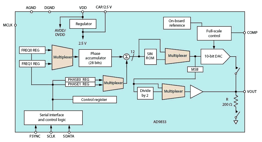 Click to enlarge |
| This direct digital synthesis IC can function as an arbitrary waveform generator by bypassing the SIN table ROM, holding the phase accumulator at zero, and using the phase register as the arbitrary-value input. |
The phase accumulator can be set to zero by first activating a software reset and then loading a zero frequency in the selected frequency register. If it then holds a constant value of zero, the DAC value is equal to that of the selected phase offset register. Thus, the phase offset register can act as the arbitrary signal input.
For the arbitrary signal generator to be useful, however, we also needed uniform timing on updates to the phase offset register—in effect, a uniform sampling rate for the DAC. We accomplished this uniform timing by leveraging the fact that data for the register comes serially (serial peripheral interface, or SPI) as 16-bit words. Taking FSYNC low enables the AD9833 to accept continual register updates (the first four bits define the register address), so every 16 bits of the serial data clock loads a new value into the phase offset register.
Therefore, after resetting the device to zero the phase accumulator, initializing the frequency register to zero, and holding FSYNC low, sending a continual stream of phase update commands results in an arbitrary waveform output with an equivalent sample frequency that is directly related to the SPI bit rate. The sample frequency is:
Sps = SCLK_FREQ / 16
where SCLK_FREQ is the SPI clock frequency at the SCLK terminal and the constant value 16 corresponds to the number of command word bits.
As an example, an SPI clock value of 12.5 MHz will result in an output sampling frequency of 0.7812 Msample/s. In practice, values higher than 1 Msample/s are easily attainable.
There are several considerations worth mentioning. One is that the phase offset registers are 12 bits wide and the DAC is only 10 bits wide, making the two least significant bits (LSBs) of the phase offset register irrelevant when creating the arbitrary waveform.
Another consideration is that the phase offset register must be loaded with a two’s complement value. Finally, the SPI clock should be related to the DDS chip’s MCLK clock, which controls the register update timing. Otherwise, the output may contain a small amount of jitter.
This direct digital synthesis IC can function as an arbitrary waveform generator by bypassing the SIN table ROM, holding the phase accumulator at zero, and using the phase register as the arbitrary-value input.