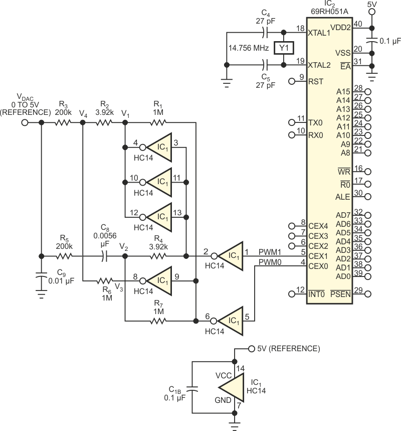
Inexpensive, 16-bit, monolithic DACs can serve almost all applications. However, some applications require unconventional approaches. This Design Idea design concerns circuitry I recently designed for a tunable-diode laser spectrometer for a Mars-exploration application. The control circuitry included two 16-bit DACs that interface to the radiation-hardened, 8051-variant 69RH051A microcontroller. Because of the intended space-flight-qualified specification, everything in the design had to consist solely of components from the NPSL (NASA parts-selection list). This restriction posed a challenge, because, at design finalization, the NPSL included no appropriate, flight-qualified, 16-bit DACs, and the budget included no funds for certification of new devices. I escaped from this impasse by exploiting two fortuitous facts: The update rate of the two DACs was only tens of hertz, and the 69RH051A had a number of uncommitted, 8-bit, 14.5-kHz PWM outputs. These outputs made one 16-bit DAC; a second pair of PWM bits and an identical circuit made the other (Figure 1).
 |
||
| Figure 1. | Two PWM outputs from a microcontroller combine to form a monotonic 16-bit DAC. | |
Hex inverter IC1's VCC rail connects to a precision 5 V reference. The inverter's outputs are accurate analog square waves. The low-order PWM-signal output, PWM0, of the 8051 controls the V3 square wave, and the high-order PWM output, PWM1, controls the V1 square wave. R2 and R6 passively sum the two square waves in the ratio R2/R6=3290/1 million=1/255 to produce V4, duplicating the 28 ratio of the 16-bit sum. This action makes the dc component of V4 equal to 5V(REF)(PWM0+255PWM1)/256. Thus, if you write the 0 to 255, high-order byte of a 0 to 65,535, 16-bit DAC setting to the CEX1 register of the 8051 and write the 0 to 255, low-order byte to CEX0, a corresponding 16-bit analog representation appears in the dc component of V4. The accuracy of the R2-to-R6 ratio is the only limit on the monotonicity and accuracy of this circuit. For example, one part in 25,500=14.5 bits for 1%-tolerance R2 and R6 and a full 16 bits for 0.3% tolerance or better. But the story doesn't end there. Two problems remain.
The first problem is the extraction of V4's desired dc component from all – or at least 15 or 16 bits=99.995% – of the undesired square-wave ac ripple. The R3-C9 lowpass filter does some of this work. If you make C9 large enough, in principle, the filter could do the whole job. The reason this simple approach wouldn't work is that, to get such a large ripple attenuation of approximately 90 dB with a single-stage RC filter would require an approximately 300-msec time constant and a resultant 3-sec, 16-bit settling time. This glacial response time would be too slow even for this undemanding application. To speed things, the R4, R5, R7, C8 network synthesizes and then sums V2: an inverse-polarity duplicate of V4's 14.5-kHz ac component. This summation actively nulls out approximately 99% of the ripple. This nullifying action leaves such a small residue that an approximately 2-msec and, therefore, approximately 25-msec-settling-time R3C9 product easily erases it.
The other problem is compensation for the low, but still nonzero, on-resistance of the HC14 internal CMOS switches, so that the resistance doesn't perturb the critical R2-to-R6 ratio. This issue is of no particular concern for R6, because the R6-to-on-resistance ratio is greater than 10,000-to-1, making any associated error negligible. This situation is not the case for R2, however, in which, despite the triple-parallel gates, the R2-to-on-resistance ratio is approximately 300-to-1, which is small enough to merit attention. Load-cancellation resistor R1 provides such attention. R1 sums a current into the R2 driving node that, because it is equal in magnitude but opposite in phase to the current through R6, effectively cancels the load on the R2 drivers. This process makes the combined on-resistance approximately 100 times less important than it otherwise would be. The result is a simple, highly linear and accurate voltage-output DAC with a respectable, if not blazingly fast, settling time of approximately 25 msec. And the most important result, in this case, was a parts list with an impeccable NPSL-compliant pedigree.