Sony delivered a lecture on a back illuminated CMOS image sensor using its own laminated structure at ISSCC 2013.
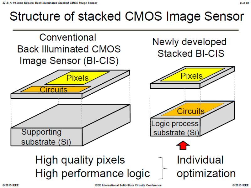
The pixel part and logic circuit part (for processing images) of the sensor, "Exmor RS," are made as separate chips and stacked by using TSVs (through-silicon vias). The pixel part and logic circuit part of Sony's previous back illuminated CMOS image sensor are formed on the same chip.
 |
| The pixel part and logic circuit part are stacked as separate chips. |
The previous sensor is attached to a silicon (Si) supporter to reduce the thickness of the chip. So, it can be said that the Si supporter was replaced with the logic chip this time.
Sony did not disclose the details of the TSV technology. But it seems that TSVs penetrating through the CMOS sensor's pixel chip are formed to connect to the logic chip after attaching the two chips together.
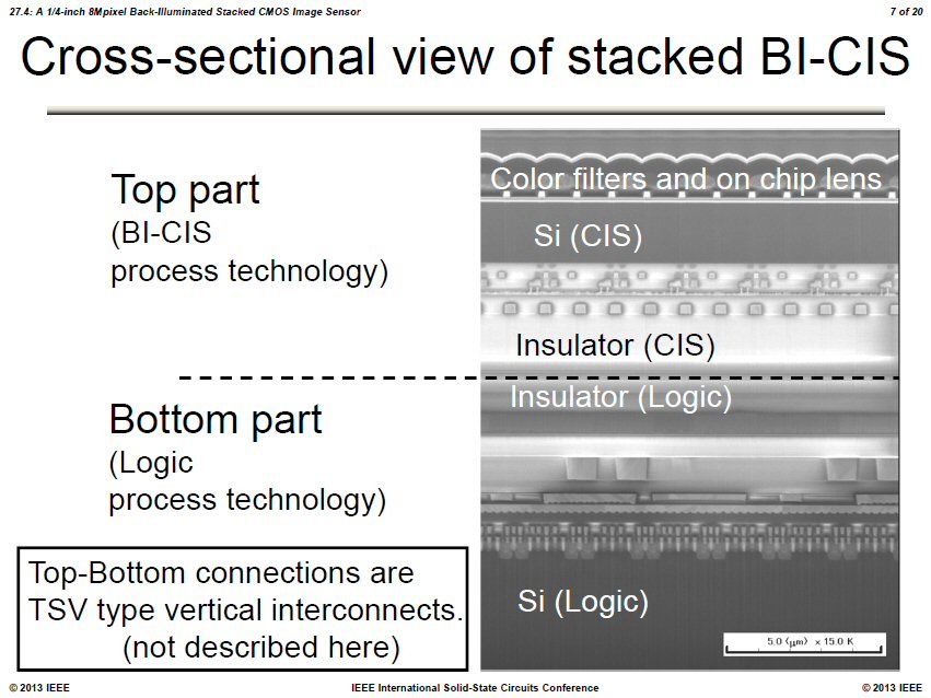 |
| The insulators of the upper and lower chips are attached together. It seems that TSVs are formed later to connect the circuit layers of the chips. |
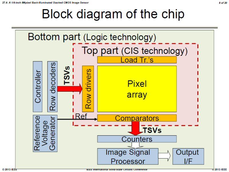
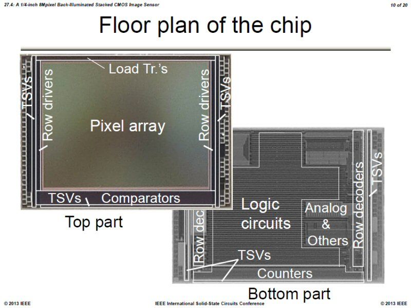
TSVs are not formed in the pixel array area. But they are used for (1) the part that connects the row drivers on the pixel chip and row decoders on the logic chip and (2) the part that connects the comparators on the pixel chip and the counters on the logic chip.
TSVs are formed on those areas to reduce the influence of noise and to make it easy to manufacture the CMOS sensor. For example, to reduce the influence of noise, comparators are arranged on the pixel chip, which can be manufactured by using Sony's matured process technology, rather than on the logic chip, the company said. The total number of TSVs is a few thousand.
 |
| The positions of the TSVs. |
By using separate pixel and logic chips, it becomes possible to use an optimal process technology for each of them. This time, Sony made the pixel chip and logic chip of the Exmor RS by using 90nm and 65nm process technologies, respectively. By stacking those chips, the company reduced chip area by 30%, compared with the previous image sensor made using 90nm process technology, while increasing the scale of the logic circuit from 500k gates to 2,400k gates.
 |
| The chips and TSVs. |
Also, because the logic chip can be manufactured at Si foundries, Sony does not have to invest in advanced logic process technologies.
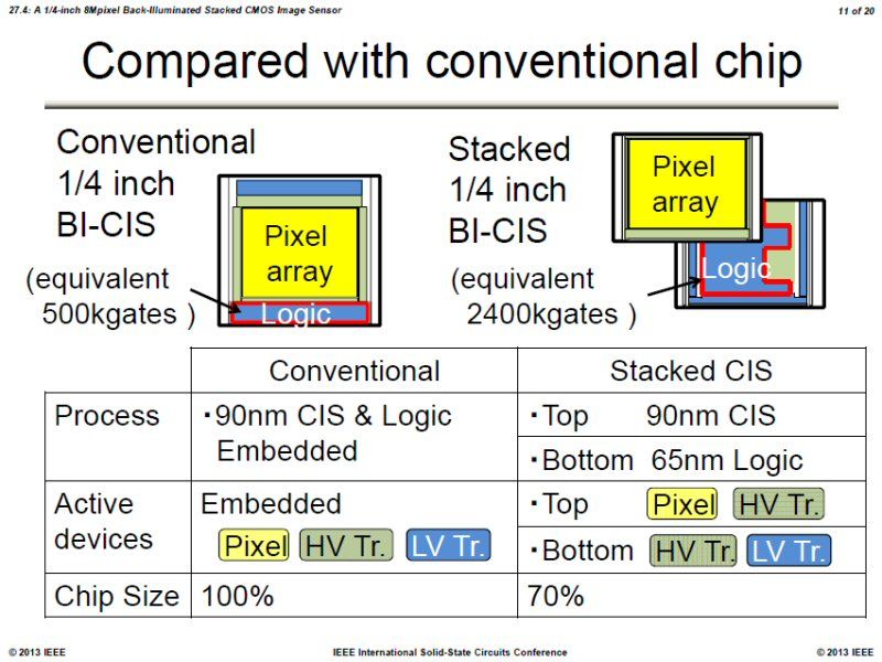 |
| Differences from the previous back illuminated CMOS sensor. |
The expanded scale of the logic circuit enabled to add various image processing functions. Specifically, it became possible to add (1) the "RGBW coding" function, which improves photographic sensitivity by adding white pixels to red, green and blue pixels and (2) the "HDR movie" function, which creates movie with a wide dynamic range by synthesizing images taken under two different exposure conditions.
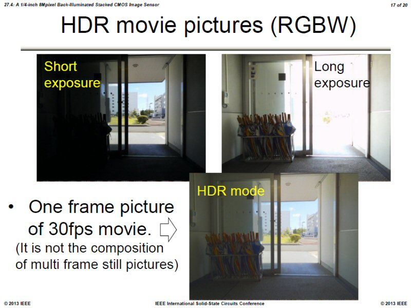 |
| Because of the expansion of the scale of the logic circuit, functions such as the "HDR movie" can be added. |
Sony has already started volume production of the new CMOS image sensor for its smartphone, other companies' tablet computers, etc. The size, pixel count and pixel pitch of the sensor are 1/4 inch, 8.08 million and 1.12μm, respectively.