Skyworks Solutions unveiled the SKY53510/80/40 family of clock fanout buffers – designed to meet the stringent timing demands of next-generation high-speed infrastructure.
With the rollout of PCIe Gen 7 and the continued expansion of AI, cloud computing, and 5G/6G networks, timing precision has become a critical enabler of performance. The SKY53510/80/40 family offers a scalable, low-jitter clock buffer solution that simplifies design and enhances signal integrity across a wide range of platforms. For system architects and hardware designers, this means faster time to market, reduced engineering overhead, and the ability to future-proof designs for emerging standards like PCIe Gen 7 and 6G wireless.
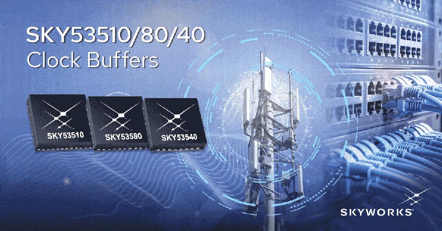
The SKY53510/80/40 family features a 3:1 input multiplexer (including crystal input), one single-ended output, and up to 10 differential outputs. Offered in compact thermally enhanced QFN packages – 7 × 7 mm (10 outputs), 6 × 6 mm (8 outputs), and 5 × 5 mm (4 outputs) – these devices are pin-compatible with industry-standard layouts for easy integration and multi-sourcing.
Designed for high-speed applications
SKY53510/80/40 buffers are well suited for:
- PCIe Gen 3 through Gen 7
- 56G/112G/224G SerDes
- 5G/6G mMIMO radio systems
- SyncE and broadcast video
- Medical imaging and aerospace/defense
These devices support input clock slew rates down to 0.75 V/ns and output levels of 1.8 V, 2.5 V, and 3.3 V – enabling robust PCB designs with minimal signal integrity challenges such as reflection, crosstalk, and ground bounce.
Key features
The SKY53510/80/40 features include:
- Ultra-low additive RMS phase jitter: 35 fs at 156.25 MHz, 3 fs at 100 MHz (PCIe Gen 7)
- Universal format translation: LVPECL, LVCMOS, LVDS, HCSL, CML, SSTL, HSTL, and AC-coupled single-ended inputs; selectable LVPECL, LVDS, HCSL, or tristate outputs
- Low power operation: Separate core/output voltage supplies (1.8 V, 2.5 V, 3.3 V)
- Integrated LDOs: >70 dBc PSRR for noisy environments
- Wide temperature range: –40 °C to +95 °C ambient (–40 °C to +105 °C board)
- Low noise floor: –166 dBc/Hz for SyncE 156.25 MHz applications
The devices are ideally suited for pairing with Skyworks’ Si551x Network Synchronizers, SKY63104/5/6 family of Jitter Attenuating Clocks and SKY62101 Ultra-low Jitter Clock Generators to deliver complete clock tree solutions that meet the demanding requirements of next-generation 6G wireless infrastructure, 800G/1600G networking infrastructure, and AI data center applications that utilize 112G/224 PAM4 SerDes technology.
Availability
Samples and production quantities of the SKY53510/80/40 clock buffers are available now. Evaluation is supported via the SKY53510-EVB development kit.
 |
| The SKY53510-EVB development kit. |