MEMS is an emerging technology which uses the tools and techniques that were developed for the Integrated Circuit industry to build microscopic machines. These machines are built on standard silicon wafers.
The real power of this technology is that many machines can be built at the same time across the surface of the wafer, with no assembly required. Since it is a photographic-like process, it is just as easy to build a million machines on the wafer as it would be to build just one.
These tiny machines are becoming ubiquitous, and are quickly finding their way into a variety of commercial and defense applications.
There are several different broad categories of MEMS technologies, outlined below:
Bulk Micromachining:
Bulk micromachining is a fabrication technique which builds mechanical elements by starting with a silicon wafer, and then etching away unwanted parts, and being left with useful mechanical devices. Typically, the wafer is photo patterned, leaving a protective layer on the parts of the wafer that you want to keep. The wafer is then submersed into a liquid etchant, like potassium hydroxide, which eats away any exposed silicon. This is a relatively simple and inexpensive fabrication technology, and is well suited for applications which do not require much complexity, and which are price sensitive.
 |
| Pressure sensor for high-rel avionics and industrial applications |
Today, almost all pressure sensors are built with Bulk Micromachining. Bulk Micromachined pressure sensors offer several advantages over traditional pressure sensors. They cost less, are highly reliable, manufacturable, and there is very good repeatability between devices.
All new cars on the market today have several micromachined pressure sensors, typically used to measure manifold pressure in the engine.
 |
| ST MEMS pressure sensor |
The small size and high reliability of micromachined pressure sensors make them ideal for a variety of medical applications as well.
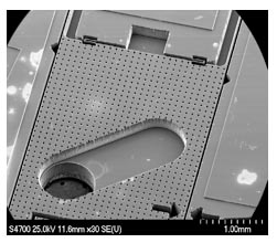
Surface Micromachining:
While Bulk micromachining creates devices by etching into a wafer, Surface Micromachining builds devices up from the wafer layer-by-layer.
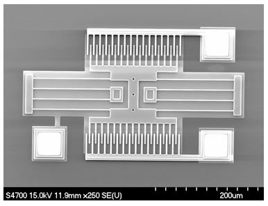 |
| Polysilicon resonator structure fabricated using a surface micromachining process |
A typical Surface Micromachining process is a repetitive sequence of depositing thin films on a wafer, photopatterning the films, and then etching the patterns into the films. In order to create moving, functioning machines, these layers are alternating thin films of a structural material (typically silicon) and a sacrificial material (typically silicon dioxide). The structural material will form the mechanical elements, and the sacrificial material creates the gaps and spaces between the mechanical elements. At the end of the process, the sacrificial material is removed, and the structural elements are left free to move and function.
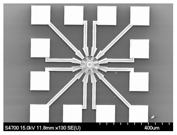 |
| Polysilicon micromotor fabricated using a surface micromachining process |
For the case of the structural level being silicon, and the sacrificial material being silicon dioxide, the final "release" process is performed by placing the wafer in Hydrofluoric Acid. The Hydrofluoric Acid quickly etches away the silicon dioxide, while leaving the silicon undisturbed.
The wafers are typically then sawn into individual chips, and the chips packaged in an appropriate manner for the given application.
Surface Micromachining requires more fabrication steps than Bulk Micromachining, and hence is more expensive. It is able to create much more complicated devices, capable of sophisticated functionality. Surface Micromachining is suitable for applications requiring more sophisticated mechanical elements.
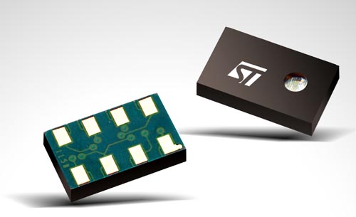
 |
| MEMS Accelerometer |
LIGA:
LIGA is a technology which creates small, but relatively high aspect ratio devices using x-ray lithography. The process typically starts with a sheet of PMMA. The PMMA is covered with a photomask, and then exposed to high energy x-rays. The mask allows parts of the PMMA to be exposed to the x-rays, while protecting other parts. The PMMA is then placed in a suitable etchant to remove the exposed areas, resulting in extremely precise, microscopic mechanical elements.
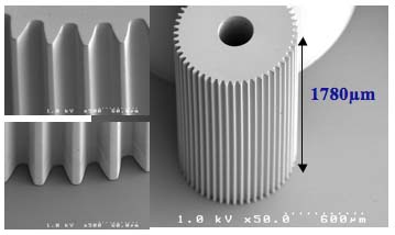 |
| A tall, high aspect ratio gear made using LIGA technology |
LIGA is a relatively inexpensive fabrication technology, and suitable for applications requiring higher aspect ratio devices than what is achievable in Surface Micromachining.
Deep Reactive Ion Etching:
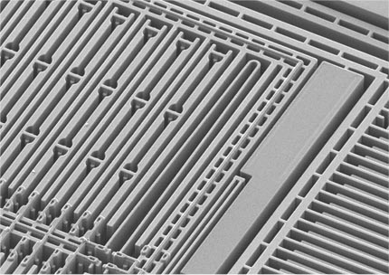
Deep reactive ion etching is a type of Bulk Micromachining which etches mechanical elements into a silicon wafer. Unlike traditional Bulk Micromachining, which uses a wet chemical etch, Deep Reactive Ion Etching micromachining uses a plasma etch to create features. This allows greater flexibility in the etch profiles, enabling a wider array of mechanical elements. The fabrication tools needed to perform Deep Reactive Ion etching are somewhat expensive, to this technology is typically more expensive than traditional Bulk Micromachining based on wet etching.
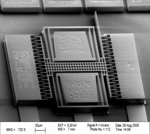
 |
| SEM of a MEMS device fabricated using two sided DRIE etching technology on an SOI wafe |
Integrated MEMS Technologies
Since MEMS devices are created with the same tools used to create integrated circuits, in some cases it is actually possible to fabricate Micromachines and Microelectronics on the same piece of silicon. Fabricating machines and transistors side by side enables machines that can have intelligence. A number of exciting products are already taking advantage of this capability.
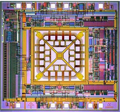 |
| MEMS-Based Accelerometer |