Some of the electrical signals we work with are said to be “floating” with respect to ground. A typical example might be a voltage drop over a shunt resistor in a power supply or a complex biomedical signal, such as an ECG. In such cases an instrumentation amplifier (IA) is used to amplify the signal’s differential mode component and reject its common mode components.
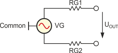
An instrumentation amplifier needs to be tested using real signals during its design, as well as periodically when in actual service. The IA should also be evaluated by applying a known, calibrated test signal to its inputs in order to determine its accuracy, common-mode signal rejection, and how it is affected by the various misconnections that can occur when it is in use. The test signal source for a medical IA should produce a suitably shaped signal UOUT with an amplitude range of few mV and a frequency range from zero to few kHz. The source should have (two) differential outputs which can be connected to the respective inputs of the IA, as shown in Figure 1.
 |
|
| Figure 1. | A differential signal source. |
The output resistances RG1 and RG2 should be, at minimum, several kΩ to simulate the characteristics of the bodies they will be measuring in real life. Additionally, both outputs should be electrically isolated from ground, but a common reference should be available for testing the IA’s ability to reject common mode interference.
Several different types of signal sources for testing are readily available. Each type, starting with function generators and ending with specialized digital synthesizers, offers a different level of precision and complexity. Many are capable of providing signals in the appropriate amplitude and frequency range, and some can even emulate ECGs, EEGs, and other medical signals. Using these sources may be challenging however, since many of them have single-ended outputs, and are not adequately isolated from ground to allow common-mode separation tests.
These sources can be adapted for testing IAs with the addition of a driver circuit that translates the single-ended signal into a differential one and ensures potential separation. This article describes the design and construction, and application of such a circuit. Its outputs are potentially separated from ground and a “common” signal is provided. In addition, the impedance of the emulated signal can be adjusted to match that of the single-ended source.
Practical optical isolation for analog signals
Isolation between the input and output is accomplished using an opto-coupler (OC), a device which contains a light emitting diode (LED) and a photodiode (PD) in the same package. The PD acts as a detector, i.e. a photoelectric current generator, where the current through the PD is proportional to the light generated by the signal passing through the LED.
For applications involving differential signals, a dual-channel OC with a single LED driving two PDs, such as Vishay’s IL300. Dual-channel devices are usually preferred to insure that any variations between the responses of the two channels (due to manufacturing variations) are kept to a minimum. In this application, the light from the LED is directed to both PDs, where one PD can be used to monitor the amount of light generated by the LED to provide a linear feedback for driving of the LED. The second PD is used to actually transmit the signal across the isolation barrier to the output. Reference 1 provides several informative examples of circuits incorporating an OC. However, all of those examples require an operational amplifier at the output side of the OC and therefore a potentially separated (isolated) power supply as well.
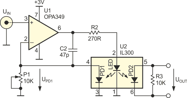
Optocouplers are typically used to provide electrical isolation for digital data streams. In these applications, they operate in “saturation mode” where the LED is driven hard enough to completely saturate the PD when it is on, and virtually no current when it is off, to produce a clean digital pulse train. In this application however, the OC is operated in its linear range, sometimes referred to as its photovoltaic mode, where the PD produces a signal that’s proportional to the light from the LED. Our DI uses the OC’s photovoltaic mode to isolate the signal generator’s analog test signals. Figure 2 illustrates a simple circuit with a linear OC, where the PDs are used in photovoltaic mode, similar to solar cells.
 |
|
| Figure 2. | A simple circuit using a linear optocoupler. |
The currents through both PD1 and PD2 are converted to voltages by the loading resistors R3 and P1. As long as both voltages (UPD1 and UOUT) remain within the linear range of the PD (less than 50 mV in our case), their amplitude will be proportional to the amount of light produced by the LED. The operational amplifier U1 compares the signal UPD1 with the input signal UIN, and drives the LED to make them equal. The trimmer P1 is used to adjust the gain (UOUT/UIN) of the circuit, and capacitor C2 prevents oscillations.
The output UOUT (our test signal source) is obtained from the second photodiode PD2, and is isolated from the ground; with its internal resistance determined by R3. The photovoltaic mode is not normally used with a linear OC, since the available output voltage range is limited to few mV. With this application the photovoltaic mode is preferred, since it does not require any power supply at the output of an OC and the desired output signal is small anyway.
Isolation variations for specialized requirements
The circuit from Figure 2 can output only positive voltages UOUT (since the current through LED and both PDs can only flow in one direction). The problem can be solved by adding a small positive offset to the input signal UIN, and most signal generators provide offset adjustment. However, this adds a DC bias to the output signal UOUT as well. If one can tolerate the DC-biased output, or reject the unwanted DC output by adding an RC high-pass filter with a suitable corner frequency and accept the modified frequency response, then the circuit from Figure 2 is adequate.
 |
|
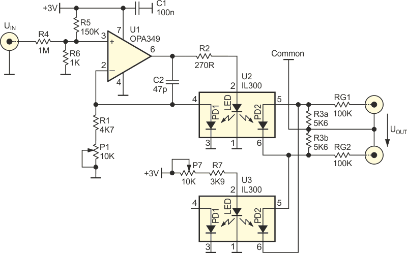
| Figure 3. | The complete schematic diagram of the optically isolated differential driver. |
If the driver’s output signal needs to be free of DC bias and its frequency response must go all the way down to 0 Hz, then the DC bias should be subtracted from the output. In this case, a second battery and a trimmer potentiometer could be used to solve the problem. However, a simpler solution that does not require a second battery is shown in Figure 3. This circuit adds a second OC (U3) which is DC driven, and its output PD is connected in anti-parallel with the output PD from OC U2. The DC current through OC U3 is set by means of P7 to compensate the bias current of OC U2.
The design also incorporates a low-power operational amplifier (OPA349), mostly because its input common mode range extends 200 mV beyond the power supply rails, and it requires very little power. As a result, the circuit’s total current consumption is about 1 mA. Since the prototype is powered two AAA batteries, it should have an operating life of close to 1000 hours.
It is important to note that the maximum range of the input signal and the circuit’s power consumption depend heavily on the bias level. The bias is fixed with the resistor divider R5/R6 to 20 mV, which sets the bias current through LED in OC U2 at roughly 500 µA. A similar LED current should be set for the OC in U3. In this variation of the original circuit, the input signal does not need to be offset from ground, due to the resistor divider comprised of R4 to R6.
The maximum acceptable input voltage (UIN) for this circuit is about ±5 V. Beyond this the output, the signal becomes distorted partially due to the low bias of 20 mV and partially due to non-linearities at the edge of the photovoltaic mode ranges of the PDs in OC U2. With 1 VPP input signal one can expect 1 mVPP output signal, and harmonics below –40 dB. The frequency response extends from 0 Hz to about 10 kHz (–3 dB).
Set up and adjustment
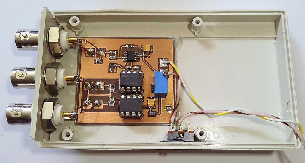
The assembled circuit is shown in Figure 4.
 |
|
| Figure 4. | The completed circuit. Note that the trimmer P1 is omitted since, in this case, it was not necessary to calibrate the gain of the circuit. |
The adjustment of the circuit starts with applying a sinusoidal signal of about 500 Hz and 4 VPP to UIN and observing the input and output (UOUT) signals using an oscilloscope. Note: the use of 10:1 probes (at minimum) is mandatory. The trimmer P1 is then adjusted to get a 1000:1 ratio in amplitudes at both traces. Finally the trimmer P7 should be adjusted to get the average output signal at UOUT to equal zero.