The article is from PCBWay website
With the continuous expansion of the application scope and application field of flexible circuit board, from the perspective of the application field of FPC and the prospect of the development law of domestic and foreign markets, FPC products are bound to be like the products of rigid printed board, and its varieties, types, structures and grades will be rapidly increased and complicated.
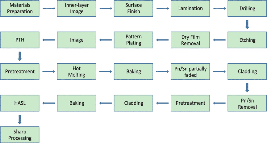
Common Double-Side Flex-PCB and Multilayer Flex-PCB Manufacturing Process:
Materials Preparation (Blanking)
The blanking content of Flex-PCB mainly includes flexible copper clad laminate, cladding layer and reinforcing plate, and the main auxiliary materials used for lamination are separation film, conformal material or silicon rubber plate, ink absorption or coated paper, etc.
Drilling
Whether it is flexible copper clad laminate or cladding layer, they are soft and thin and difficult to drill, so it is need to stack boards before drilling, that is stack-up which means that a dozen pieces of cladding layer or a dozen pieces of copper clad laminate stack together like a book together.
Desmear and Pitting
After drilling, the PCB holes’ wall may have some dirt of resin, only the dirt of the holes can be completely removed to ensure the quality of plated-through hole. The double-sided flexible copper clad laminate after drilling is generally necessary to do the desmear and pitting, and then carry out PTH.
1. PTH and Pattern Plating
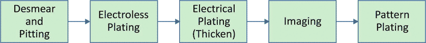
2. Electroless Plating
The pretreatment solution is preferably acidic colloid palladium rather than alkaline ionic palladium. In general, attention should be paid to both preventing the reaction time from being too long and the speed from being too fast, which will lead to the swelling of flexible materials, and the excessive speed will lead to holes and holes and poor mechanical properties of copper layer.
3. Electrical Plating
Due to the poor mechanical properties (such as ductility) of electroless copper plating layer, it is easy to break under thermal shock. So generally when the chemical copper plating layer is up to 0.3~0.5 µm, the electrical plating should immediately carry out in order to thicken the whole panel to 3-4 µm to ensure the integrity of the hole wall coating in the subsequent processing process.
4. Pre-cleaning and Imaging
Before imaging, the surface of the board must be cleaned and roughened first, and the process is roughly the same as the rigid PCB. But because flexible substrate is easy to deform and bend, it is advisable to use chemical cleaning or electrolytic cleaning. It can also use manual pumice stone wash or special pumice stone paint board machine. The process of sticking dry film, exposure and developing of flexible PCB is familiar with that of rigid PCB. The dry film after developing becomes brittle due to the polymerization reaction, and its binding force with copper foil also decreases. Therefore, the dry film after developing holds to pay more attention to prevent it from warping or peeling.
5. Etching
There are usually many long parallel wires at the bend of flexible substrates. In order to ensure the consistency of etching, it is possible to pay attention to the spraying direction of etching solution, pressure, position and transmission direction of printed board during etching. When etching, a rigid substrate should be attached to the flexible substrate in front of it to pull it forward. Finally, it is better to use the etching fluid automatic regeneration system.
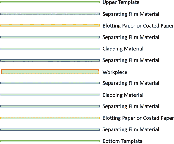
6. Position of Cladding Layer
PCBs after etching need to do surface treatment in order to increase the binding force before the process of position of cladding layer. The cladding layer after drilling and the flexible PCBs after etching have different degrees of moisture absorption. Therefore, these materials should be dried in the drying oven for 24 hours before lamination, and the height of stack-up should not exceed 25 mm.
7. Lamination
7.1 Lamination of Cladding Layer of Flex-PCB
According to different flexible substrates to determine the lamination time, heating rate and pressure and other laminating process parameters. Generally speaking, its process parameters are as follows:
- Lamination time: the net pressure time under the full pressure is 60 min.
- Heating rate: temperature need to reach 173 °C within 10 to 20 min from the indoor temperature.
- Pressure: 150-300 N/cm2, to reach the full pressure within 5-8 seconds.
7.2 Gasket Material of Lamination:
The choice of gasket material is very important to the lamination quality of flexible and rigid-flex PCB. The ideal gasket material should have good formability, low fluidity, and cooling process does not shrink, in order to ensure that no bubbles and flexible material laminate in lamination, deformation does not occur. Gasket materials are usually divided into flexible and rigid systems. Flexible system mainly includes PVC film or radiation polyethylene film and other thermoplastic materials. The rigid system is mainly made of glass cloth reinforced by silicone rubber.
8. Baking
The main purpose of baking is the removal of moisture in the processing.
9. HASL or Hot Melting
The PCB after drying should be immediately carried out the HASL or hot melting to prevent it from wetting.
10. Shape Processing
The shape processing of flexible PCB, it is the use of seamless precision steel die in the mass production, and it can be a mold a cavity, can also be a multi-cavity mold.
11. Packaging & Shipping
Flex-PCB usually cannot only use between the blocks add wrapping paper or foam pad separation, but a few boards, together up and down with foam pad vacuum packaging machine vacuum packaging, or it can also use the vacuum packaging bag with add desiccant, which can extend the storage time. PCBWay offers flexible shipping methods for our customers, you can choose any one of the methods, such as FedEx, DHL, EMS, UPS, TNT, Hongkong Post and so on.
12. Placing order in PCBWay
PCBWay offer online quotation service for flexible and rigid-flexible PCB, and their delivery time as fast as 3 days.
