Part 1
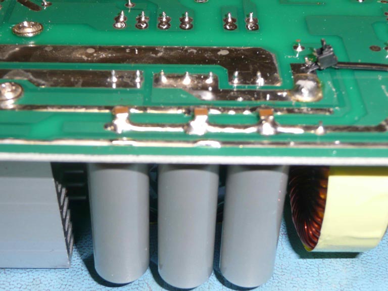
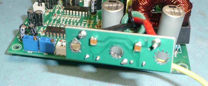
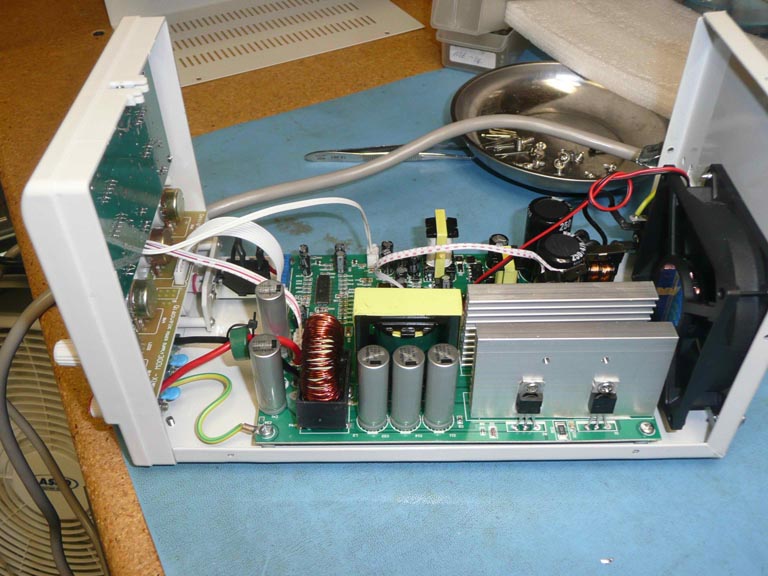
First, the filtering electrolytic capacitors that were installed in front of the inductor were replaced with better ones and with larger capacity. Initially, two electrolytic capacitors with a capacity of 330 μF × 100 V each were installed in the BPS. It’s interesting that there are places for three such capacitors provided on the printed circuit board (PCB) (see Figure 6). Instead of these two capacitors, the author installed three new ones - 430 uF × 100 V each.
Then, the leads of these capacitors were connected to ceramic capacitors, placed as close as possible to the leads of the electrolytic ones. The results of these two steps are shown in Figure 15.
 |
| Figure 15. |
New electrolytic capacitors and ceramic capacitors
at their leads. |
Next, the filter coil was replaced with another one, with a higher inductance. When analyzing the situation, the author measured the inductance of the coil installed by the manufacturer and found another one with the same footprint, but with bigger inductance. The original coil has been unsoldered and measured. There was no marking on it at all and the measured inductance was about 100 μH. A replacement was found - a high-frequency coil with the same dimensions and pin layout, but with an inductance of 400 μH. Figures 16, 17, 18 show the old and new coils and the circuit board with the new coil installed. Please note that the new coil has three leads. Lead number 3 is not connected to the coil’s winding and serves only for mechanical fastening. Therefore, the author soldered this lead to the lead of one of the resistors next to the coil to ensure mechanical strength.
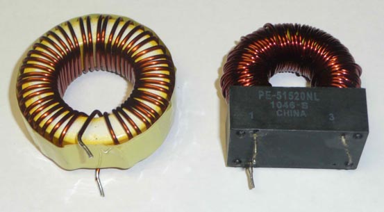 |
| Figure 16. |
Old (left) and new (right) coils. |
| |
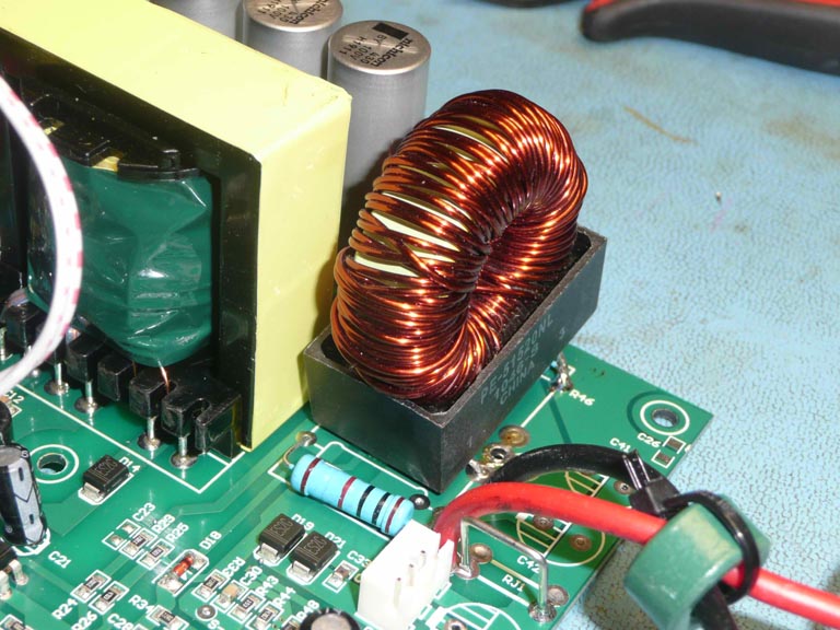 |
| Figure 17. |
A circuit board with a new coil installed. |
| |
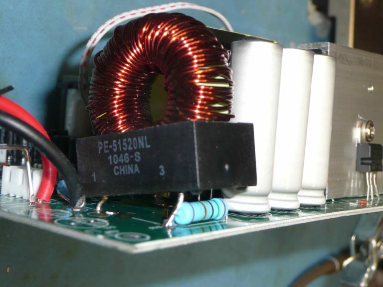 |
| Figure 18. |
A circuit board with a new coil installed. |
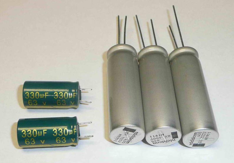
Also, filter electrolytic capacitors located behind the coil were replaced with better ones, with a larger capacity and a higher voltage. When studying the printed circuit board, it turned out that behind the inductor, the manufacturer installed two electrolytic capacitors of 330 μF and a voltage of 63 Volts each - and this is at the output of the BPS with a maximum voltage of 60 Volts. It has been decided to replace these two capacitors with other electrolytic capacitors - 430 uF × 100 V each. At first, the author was going to install three such capacitors, but in the process it turned out that there was not enough room for the three new capacitors, since they were larger in diameter than the old ones. Therefore, behind the inductor, only two capacitors were installed. And also, as in front of the coil, a shunt ceramic capacitor was installed on the leads of each electrolytic capacitor. Several such ceramic capacitors have also been added between the output traces of the printed circuit board. New and old electrolytic capacitors, installed new electrolytic capacitors and ceramic capacitors are shown in Figures 19, 20, 21.
 |
| Figure 19. |
Old (on the left) and new (on the right) electrolytic capacitors. |
| |
 |
| Figure 20. |
Old (on the left) and new (on the right) electrolytic capacitors. |
| |
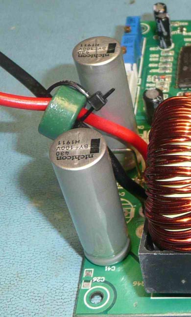 |
| Figure 21. |
Installed new electrolytic capacitors. |
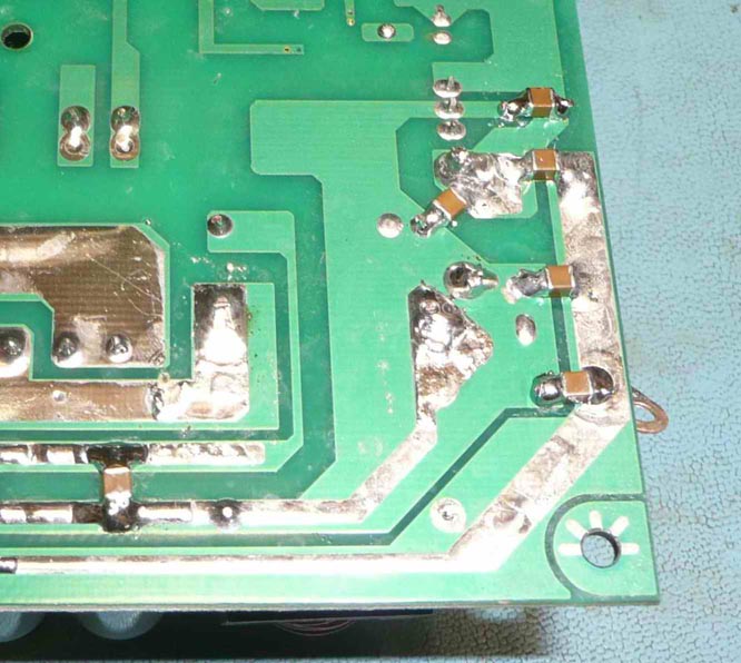
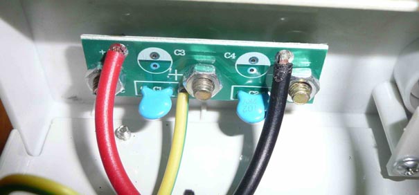
And at the end, the shunting of the leads of the output terminals with ceramic capacitors was performed. Upon a detailed examination of the output terminals, it became clear that there was a place for electrolytic capacitors on a separate printed circuit board to which these terminals are attached, apparently, according to the footprint, not of a large capacity, but which were not installed. Therefore, on the reverse side, two shunt ceramic capacitors were added to the pads of these non-installed capacitors. The appearance of this circuit board before and after the modification is shown in Figures 22 and 23.
 |
| Figure 22. |
Output terminals printed circuit board before modification. |
| |
 |
| Figure 23. |
Output terminals printed circuit board before modification. |
Having all these steps completed, the BPS has been assembled, using better screws, solder, flux and using of heat shrink insolation for all AC wires.
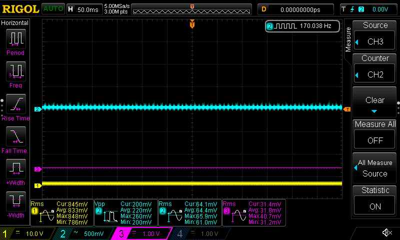
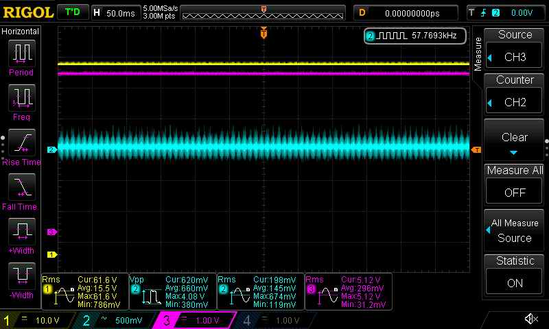
After the unit has been assembled (but top cover was not installed just yet), it was time to test BPS again. We turn it on and check the BPS after modification, using the same testing setup. Test results after modification are shown in Figures 24,25,26,27
 |
| Figure 24. |
BPS after modification, in IDLE mode. The output voltage control is set to minimum. |
| |
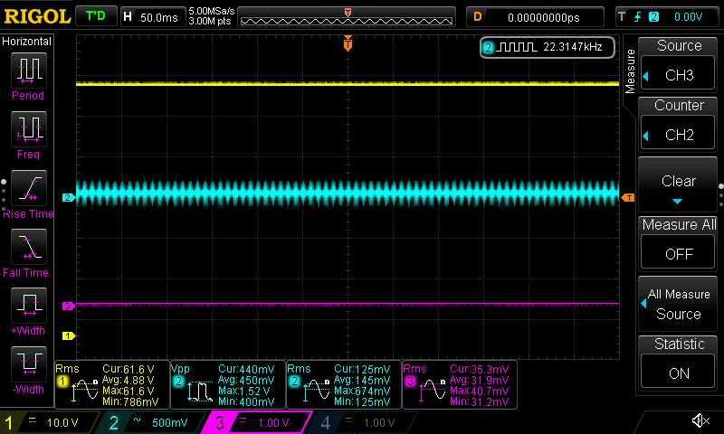 |
| Figure 25. |
BPS after modification, in IDLE mode. The output voltage control is set to maximum. |
| |
 |
| Figure 26. |
BPS after modification, under load. The output voltage control is set to minimum. |
| |
 |
| Figure 27. |
BPS after modification, under load. The output voltage control is set to minimum. |
The assembled BPS after modification (without the top cover) is shown in Figure 28.
 |
| Figure 28. |
BPS after modification, without a top cover. |
Comparison table of BPS test results before and after modification.
| Table 1. |
Comparative table of BPS testing results before and after modification. |
| |
|
Before Modification |
After Modification |
| |
|
Vpp |
Vrms |
Vpp |
Vrms |
| Idling |
Output Voltage
Is Minimum |
820 mV |
210 mV |
220 mV |
65 mV |
Output Voltage
Is Maximum |
1.27 V |
355 mV |
450 mV |
145 mV |
Under
Load |
Output Voltage
Is Minimum |
820 mV |
210 mV |
205 mV |
58 mV |
Output Voltage
Is Maximum |
1.7 V |
545 mV |
660 mV |
145 mV |
|
The author modified four such BPSs as described above. All four units after modification showed much lower high-frequency noise level at the output both in idle mode and under maximum load.
Conclusion: if this BPS is planned to be used to power electronic devices, it is not advisable to do this without modification due to the high level of high-frequency noise and ripples at the BPS output. This high-frequency noise can be significantly reduced by following all the steps described above.
List of components used in the project:
- Electrolytic Capacitors - MPN: UBY2A431MHL
430 µF 100 V Aluminum Electrolytic Capacitors Radial, Can 31 mOhm @ 100 kHz 3000 Hrs @ 135 °C
- Ceramic Capacitors - MPN: GRM32DC72A475KE01K
4.7 µF ± 10% 100 V Ceramic Capacitor X7S 1210 (3225 Metric),
- RF choke - MPN: PE-51520NL.