Question:
Where should the coil go?
Answer:
Switching regulators for voltage conversion use inductors for temporarily storing energy. These inductors are often very large components and must be positioned in the printed circuit board (PCB) layout of the switching regulator. This task is not that hard because the current through an inductor can change, but not instantaneously. There can only be continuous, usually relatively slow changes.

Switching regulators switch the current flow back and forth between two different paths. This switching occurs very rapidly and the speed depends on the switching edge durations. The resulting traces, which conduct current in one switching state and do not conduct current in the other switching state, are called hot loops or ac current paths. They should be kept especially small and short in the PCB layout so that parasitic inductance is minimized in these traces. Parasitic trace inductances generate an undesired voltage offset and result in electromagnetic interference (EMI).
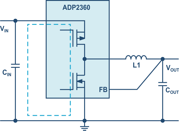
Figure 1 shows a step-down regulator in which the critical hot loop is shown as a dotted line. It can be seen that coil L1 is not part of the hot loop. Thus, it can be assumed that placement of this inductor is not critical. It is correct to have the inductor lie outside the hot loop – therefore placement is, in the first instance, secondary. Still, a few rules should be followed.
 |
||
| Figure 1. | A switching regulator for step-down conversion with a critical hot loop shown as the dotted line. |
|
No sensitive control traces should be routed under an inductor, neither right on the PCB surface nor below, in internal layers, or on the backside of the PCB. Due to the flow of current, the coil generates a magnetic field, which can affect weak signals in a signal path. In a switching regulator, one of the critical signal paths is the feedback trace, which connects the output voltage to the switching regulator IC or to a voltage divider.
It should also be noted that a real coil has a capacitive effect as well as an inductive one. The first coil windings are directly connected to the switch node of a step-down switching regulator, as shown in Figure 1. As a result, the voltage changes just as strongly and rapidly as the voltage at the switch node does. With very short switching times and high input voltages in the circuit, a considerable coupling effect is yielded on other paths on the PCB. Thus, for this reason as well, sensitive traces should be kept away from the location of the coil.
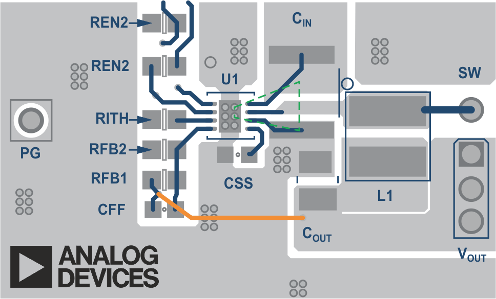
Figure 2 shows a sample layout with the ADP2360. Here, the important hot loop from Figure 1 is marked in green. The yellow feedback path can be seen at a distance to coil L1. It is on an internal layer of the PCB.
 |
||
| Figure 2. | Example circuit with an ADP2360 step-down (buck) converter with coil placement. |
|
Some circuit designers even go so far as to not want any copper layers in the PCB under the coil. They would, for example, provide for a cutout under the inductor, even in a ground plane layer. The goal is to prevent eddy currents in the ground plane under the coil resulting from the magnetic field of the coil. This approach is not wrong, but there are arguments for a solid ground plane with no interruptions:
- A ground plane for shielding works best when it is not interrupted.
- The more copper a PCB has, the better the heat dissipation is.
- Even if eddy currents are generated, these currents flow locally, only cause small losses, and hardly affect the function of a ground plane.
Thus, I am in favor of a solid ground plane layer, even under the coil.
In summary, we can conclude that the coil of a switching regulator is not part of the critical hot loop, but that it makes sense to not route control traces under or very close to the coil. Various planes on the PCB – for example, for ground, or also for VDD (supply voltage) – may be created continuously, without cutouts.