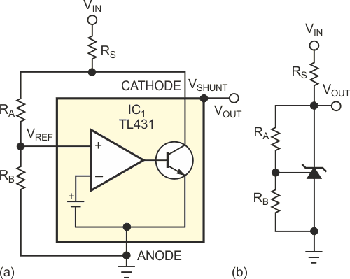
The popular and multiply sourced TL431 three-terminal shunt regulator offers designers considerable versatility in its applications. Figure 1a illustrates the TL431’s internal circuitry, which comprises a precision voltage reference, an operational amplifier, and a shunt transistor (Reference 1). In a typical voltage-regulator application, two external resistors, RA and RB, determine the shunt-regulated output voltage at the lower end of load resistor RS (Figure 1b).
 |
|
| Figure 1 | An uncomplicated block diagram (a) conceals the TL431’s internal complexity, but you need only three external resistors to use the TL431 in a basic shunt-regulator circuit (b). |
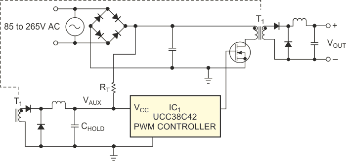
By way of illustration, the TL431 and a few external active and passive components can serve as a low-power auxiliary power supply for an SMPS (switched-mode-power-supply) PWM (pulse-width-modulated) controller. In some power-supply designs, an auxiliary winding on the step-down transformer supplies power to the PWM controller. Under light output loads, the auxiliary winding may supply inadequate power to the PWM controller.
For example, the converter circuit in Figure 2 derives power for PWM controller IC1 through an auxiliary bias winding, WAUX, which is part of transformer T1. Resistor RT and capacitor CHOLD form a trickle-charge circuit that supplies start-up power to IC1. To conserve energy, resistor RT supplies just enough current to trickle-charge CHOLD to voltage VAUX. Once the circuit starts, it operates as you would expect and delivers output power to the load, and the auxiliary winding and its components power the PWM controller.
 |
|
| Figure 2 | An auxiliary winding supplies power to the supply’s PWM controller. |
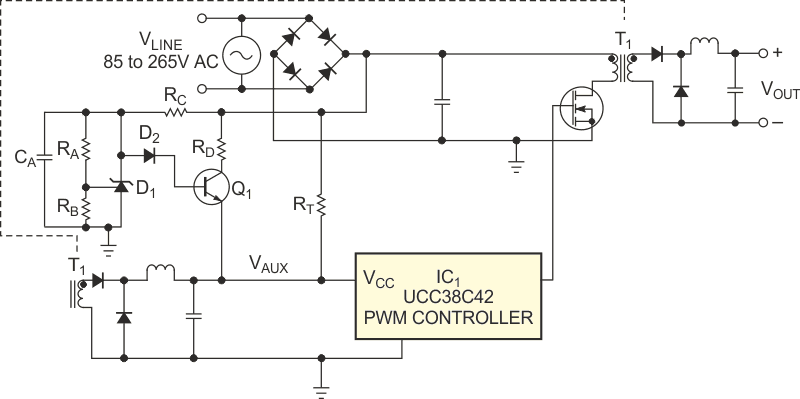
However, removing the output load reduces the energy supplied to the auxiliary bias winding, depleting the charge on CHOLD and causing IC1 to turn off, which in turn upsets output-voltage regulation and causes the power supply to operate erratically. A low-power bias-supply circuit supplies light-load start-up power and then switches off to conserve power whenever the auxiliary winding can supply enough energy to PWM controller IC1 (Figure 3). In this circuit, a series-pass regulator turns on under light-load conditions and turns off when the bias winding can supply the energy to the PWM controller, thus conserving energy under load and improving converter efficiency.
Resistors RA through RD, shunt regulator IC1, diode D1, and transistor Q1 form the low-load series-pass-regulated bias supply. You select these components to produce a voltage at Q1’s emitter that falls between IC1‘s turn-off voltage and the nominal voltage produced by rectifying the auxiliary bias winding’s output, VAUX_NOM. In effect, the voltage at IC1‘s VCC pin follows in wired-OR fashion whichever is higher: VAUX_NOM or the voltage at transistor Q1‘s emitter. When the auxiliary bias winding and its components deliver sufficient power, Q1‘s emitter sees a reverse bias, and Q1 shuts off to conserve energy. Conversely, Q1 supplies power when VAUX decreases below VAUX_NOM due to a light output load. Note that the circuit still must include trickle-charge resistor RT because most PWM controllers incorporate undervoltage lockout, the ability to start at a higher than nominal supply voltage.
 |
|
| Figure 3 | In this improved design, pulse-width-controller IC1 derives its power from RT for start-up, auxiliary winding WAUX for normal operation, and shunt-regulator circuit IC2 and Q1 for low-load operation. |
To design the series-pass regulator, select resistor RC to supply sufficient operating current to IC2, and select resistor RD to maintain Q1‘s collector voltage and current within its safe operating area. Select resistors RA and RB to set the series regulator’s output voltage above IC1’s start-up voltage and below the nominal voltage supplied by the auxiliary winding’s rectified output. Choose bypass capacitor CA to minimize ripple voltage across IC2.
You can use the following equation to adjust the voltage divider formed by resistors RA and RB:
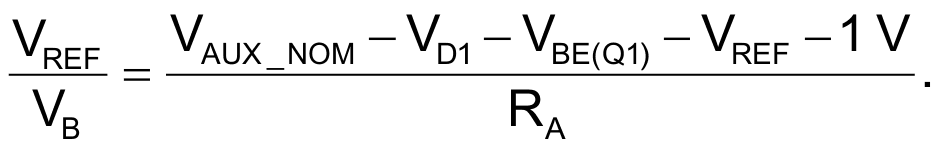
The voltage at Q1’s emitter must fall below the nominal auxiliary voltage, which the auxiliary bias winding supplies. VREF represents shunt regulator IC2’s internal nominal reference voltage of 2.495 V, and VD1 and VBE(Q1) represent D1’s voltage drop and Q1’s forward base-emitter voltage, respectively.