It may be hard to believe, but 2022 marks flash memory's 35th anniversary. Time, it appears, flies particularly quickly when a technology becomes as essential and widely adopted as flash storage (Fig. 1).
 |
|
| Figure 1. | Flash memory growth in all areas has been significant over the last 35 years. |
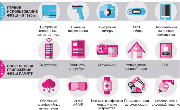
Since its creation in 1987, flash memory has become a fundamental storage technology, widely used in mobile devices, business and personal computers, digital cameras, scientific research equipment, electronic musical instruments, medical devices, spacecraft, automotive and aviation systems, and a virtually endless array of other systems and devices (Fig. 2).
 |
|
| Figure 2. | The number of flash storage applications have grown along with the size, capacity, and performance. |
Both NOR and NAND types of flash memory were invented by Toshiba's semiconductor business division (since renamed KIOXIA). The original device was named "a simultaneously erasable EEPROM." The flash name was later substituted because the device could erase a large number of memory cells simultaneously in a “flash." Unlike dynamic random-access memory (DRAM) chips, non-volatile flash devices retain stored information even after power is switched off.
NAND Replaces NOR
The original NOR device, while a breakthrough technology, was limited in size and cost. NAND, meanwhile, supplied a configuration with a reduced memory cell area that allowed a lower per-bit cost.
Despite its great potential, flash was hardly an overnight sensation. In fact, some industry detractors quipped that flash was a technology in search of a problem. Things got so bad that at one point, KIOXIA’s predecessor (Toshiba) even considered halting the project. It seemed like a reasonable option at the time, since after three years of commercial availability, NAND flash had yet to attract any paying customers.
The Tide Turns
In the 1990s, NAND flash began finding its markets – and customers. Adoption picked up speed when manufacturers of digital telephone answering machines, barcode readers, digital cameras, and MP3 players began recognizing that NAND flash was a perfect storage technology for their products.
As the decade dawned, Toshiba and SanDisk agreed to jointly develop and manufacture gigabit-scale flash memories. The industry's first NAND flash joint venture paved the way toward today's "megafab" facilities. Large-scale production lowered the cost per gigabit, leading to the use of NAND flash storage in a wider range of products.
Things really shifted into high gear in 2001, when a transition from single-level-cell (SLC) to multi-level-cell (MLC) technology opened the way to enabling high-volume production, increased densities, and lower cost per bit.
In 2005, Fab 3, a 300-mm NAND flash megafab, was built to meet the growing demand for flash memory in digital consumer devices, including mobile phones and digital still cameras. High-volume production lowered the cost per gigabit, leading to the use of NAND flash storage in an even wider range of products.
Also, in 2005, 8-Gb NAND flash memory chips arrived, ushering in a new era of 1-GB data storage capacity on a single chip. The chips utilized MLC technology that allowed for two bits of data to be stored in a single memory cell, effectively doubling memory capacity. NAND flash was soon introduced into notebook and desktop computers, providing speed, space, weight, and power savings over hard-disk-based storage.
In 2007, 3D flash memory technology was announced. The event was highlighted by a paper presented by Toshiba (now KIOXIA), which introduced BiCS FLASH 3D flash memory at that year's IEEE VLSI Symposium.
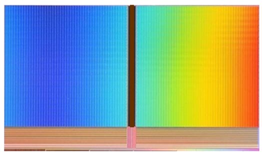
Continuing the refinement of its BiCS FLASH technology, KIOXIA 512-Gb 3D flash memory (Fig. 3) featured the industry’s largest capacity. It led to the creation of a 1-TB product with a 16-die stacked architecture in a single package, enabling more density per layer – and kicking off a "layers race."
 |
|
| Figure 3. | BiCS FLASH 3D technology delivered 512 Gb of NAND flash memory. |
Impressive Advances
Even after 35 years, the flash memory story is continuing to progress rapidly. Breakthrough quad-level-cell (QLC) technology, for example, provides significantly expanded capacity by pushing the bit count for data per memory cell from three to four.
Overall, flash memory has come a long way over a remarkably short time span. The technology has notched impressive advances in price per gigabyte ($10,000 in the 1990s to approximately $0.20 today – a 50,000X decrease), and an equally imposing increase in die density (4 Mb in the 1990s to 1.33 Tb today).
Similar progress has been made in media storage. In music, flash memory has advanced from the minuscule one-sixteenth of a song that could be stored on a 4-Mb NAND die to the 20,000 songs that can fit on a 1.33-Tb NAND die.
Moving Forward
Today's flash-enabled applications are profuse and ever-growing. The technology is now moving into new fields, such as cloud/edge computing, industrial automation, gaming-oriented AR/VR devices, wearable/digital health devices, AI, and many other cutting-edge systems and products.
In just 35 years, flash has evolved from a "solution looking for a problem" into a $70 billion market. If the past is any indication, flash memory's remarkable journey will continue far into the future.