Fujitsu Semiconductor limited announced that it has developed the world's first technology to produce chips with embedded flash memory on logic circuits fabricated using deeply depleted channel (DDCTM) technology, with the 55nm process at the company's Mie Plant. This makes it possible to consolidate DDC—for low-power operation in a conventional CMOS design—with flash memory, which is non-volatile memory, on a single chip, opening up new possibilities for a wide range of applications, such as the Internet of things. Details of this development will be presented at the IEEE International Electronic Device Meeting (IEDM) 2013.
As the Internet of things—in which many kinds of devices are connected to each other via the Internet—becomes more common, there is likely to be a growing demand for devices such as LSIs with built-in sensors for use in wireless sensor networks. For applications such as these, in addition to the necessary characteristics of low-voltage operation and low power consumption, there is demand for device equipped with non-volatile memory, which does not require power for storing sensor data.
Fujitsu Semiconductor licensed technology from SuVolta, Inc., and then worked on co-developing the world's first practical implementation of low-power DDC technology. Production of these chips has already begun at Fujitsu Semiconductor's Mie Plant. Fujitsu Semiconductor has developed a fabrication technology that makes it possible to consolidate DDC transistors on the same chip with floating-gate tunnel oxide (FLOTOX) flash memory.
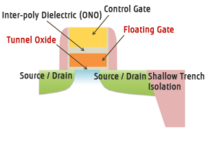
In FLOTOX flash memory (Figure 1), inserting electrons into a floating gate (program), and extracting electrons from it (erase), are used to represent the 0s and 1s of data. When inserted electrons leak out of the floating gate, it becomes impossible to store data correctly. Indeed, the "single bit charge loss" (SBCL) that can occur after repeated program/erase cycles is the greatest challenge when using this design. It had been thought that steps such as "STI corner rounding" and "tunnel oxide formation" used in FLOTOX fabrication need to be processed at high temperatures (approximately 1.000 °C) in order to avoid this failure.
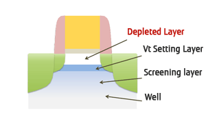
DDC transistors (Figure 2), however, are characterized by the formation of the depleted layer, where dopants are held to very low density, underneath the gate electrode. The use of high-temperature processes is incompatible with the formation and retention of this kind of layer.
Fujitsu Semiconductor's development team focused on forming FLOTOX using only low-temperature processes. They conducted a complete review, paying close attention to each process along the way, and found that adjustments that would optimize the dopant density distribution in the channel region and source/drain electrodes would result in process conditions that can form FLOTOX structures, while maintaining the characteristics that DDC transistors require. Test chips produced with these new parameters were confirmed to have good initial characteristics for flash-memory operation and to be free from SBCL failures after repeated program/erase cycles, demonstrating that it is free from reliability problems.
Furthermore, in the course of this optimization work, it was found that the mechanism that produces SBCL is not current stress on the tunnel oxide film, as previously believed, but is dictated by hot hole injection near drains. This new understanding is likely to contribute to further process optimizations in the future.