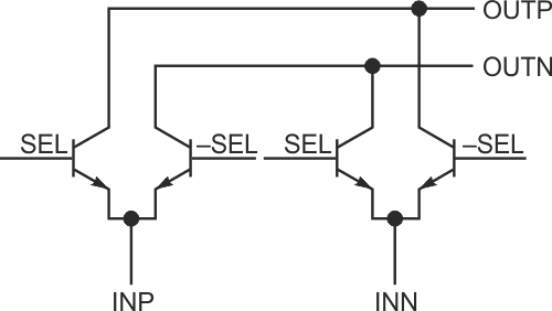
You can effectively double the sample rate of a DAC by interleaving two DACs into a single unit. Updating each DAC on an alternating basis and switching to the appropriate output double the effective throughput of the overall system. It is essential to overall performance that you use a high-quality, high-speed switch in the multiplexing of the DACs' outputs. The current-mode DACs in this Design Idea allow for current-steering implementation of the output switch. Current steering uses two differential-transistor pairs cross-coupled in the form of a four-quadrant multiplier (Figure 1). In this topology, the saturation voltages of the transistors are minimal, voltage swings are small, and switching speeds are high.
 |
|
| Figure 1. | You can use cross-coupled differential transistor pairs as current-mode switches. |
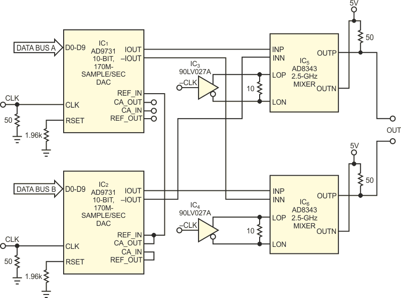
The 2.5-GHz AD8343 mixer contains a complete four-quadrant-multiplier structure that you can use as a high-speed, current-mode switch. The bias circuitry internal to the AD8343 sets the dc voltage at the emitters to approximately 1.2 V, which in turn sets the compliance voltage necessary at the DAC outputs. With only a minimal drive signal at the base connections, the emitters appear as a virtual ac ground. The reduced voltage swing at these nodes minimizes the effect of any parasitic capacitances. This Design Idea uses two AD8343 mixers as high-speed switches to multiplex the differential output currents derived from two AD9731 DACs (Figure 2).
 |
|
| Figure 2. | “Ping-ponging” the outputs of two DACs effectively doubles the throughput rate. |
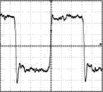
On the output side of the mixers, the termination resistors allow for a dc path to the supply, provide for the current-to-voltage conversion, and present a single-ended back-termination impedance of 50 Ω. This configuration allows the circuit to drive a remotely located, 100 Ω, differential load via two 50 Ω coaxial cables. The low-level clock signals at the LO inputs come from high-speed LVDS buffers terminated in resistances of 10 Ω. The approximate ±3.5-mA p-p drivers produce roughly 70-mV p-p drive at the LO inputs. Figure 3 shows that the circuit provides output rise and fall times faster than 200 psec.
 |
|
| Figure 3. | The circuit in Figure 2 produces outputs with less-than-200-psec rise and fall times. |