Boost converters, like other switchers, have traditionally received their control signals from a dedicated circuit. However, a recent trend is to integrate simple switching-power-supply building blocks into generic devices, such as microcontrollers. An excellent example of this concept is a microcontroller that combines digital and analog circuitry and makes it easier to build simple power supplies. The programming capability of a microcontroller is an added benefit in power-supply designs, especially when you want to experiment with the supplies.
 |
|
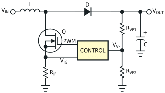
| Figure 1. | This circuit block represents the basic topology of a boost converter. |
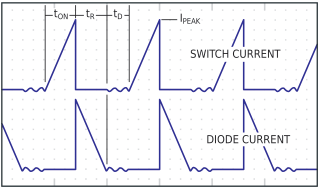
Figure 1 illustrates a simple boost-converter design using a microcontroller; the basic boost topology in Figure 1 is a type of flyback circuit. The basic concept is easy to understand. When the MOSFET, Q, turns on, the current flowing through the inductor, L, begins to ramp up linearly (Figure 2), resulting in energy storage in the inductor. The MOSFET turns off before the inductor saturates. At this time, the inductor releases its energy to the storage capacitor, C, and the load.
 |
|
| Figure 2. | These curves show the switch and diode currents in the circuit of Figure 1. |
You can design a simple boost converter with the following conditions:
VIN = 9 V,
VOUT = 18 V,
RLOAD = 72 Ω,
F = 1/T = 62.5 kHz,
η = 70%,
ΔVDROP = 50 mV,
where F is the switching frequency, η is the efficiency, and ΔVDROP is the output ripple voltage.
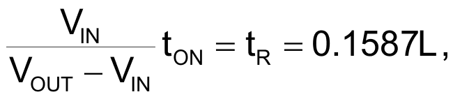
You can calculate the on-time, current, ramp-down time, and the total period in terms of inductance:


Then, you calculate the peak current through the inductor and the inductance value:


Finally, you calculate the capacitance based on the ripple voltage:
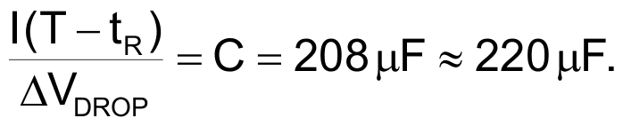
Note that the design is slightly altered to use readily available components, by using a 33-µH inductor and a 220-µF capacitor. The difference in the inductor value is absorbed in the dead time, as is the power loss.
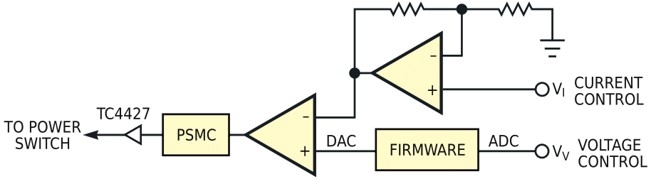
The control circuit can take many forms, especially if you choose a device such as the PIC16C782 microcontroller. This device integrates a built-in analog peripheral set, diverse analog visibility, and a mixed-signal PWM block. The control circuit in Figure 3 demonstrates how the analog and pulse-width modulation is contained within the PIC16C782, with the exception of the FET driver. This control circuit combines analog current control and firmware voltage control. The interesting part is the firmware, which is directly in the voltage-feedback path of the control loop. Through firmware, you can alter the dynamics of the control loop by changing the functions within the program. You may be able to design an adaptive power-control system by adjusting the phase and gain to meet the desired needs of a system.
 |
|
| Figure 3. | A microcontroller contains all the elements necessary for boost-converter control. |
Firmware placement within the control loop is not the only possibility; you could use a combination of firmware and hardware to monitor the system. Because the analog information is visible and the analog functions are controllable within the PIC16C782 device, you can monitor an active system for performance and function. In essence, the system can have self-diagnostic capabilities to check stability, load, input and output conditions, or anything else a system may require. You can also obtain Information about the system, through a serial port or some other means, by routing the data to a terminal or computer display. Even better, the firmware allows the design to change the functions without changing hardware. This approach eases experimentation; you simply changing firmware rather than spending hours in the lab adding or changing parts.
 |
|
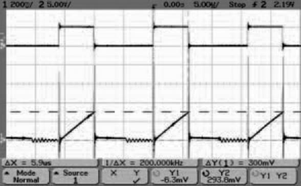
| Figure 4. | A working example of the boost converter implementing the basic topology of Figure 1 shows the duty cycle (top) and the current-ramp- down waveform (bottom) for the circuit in Figure 1. |
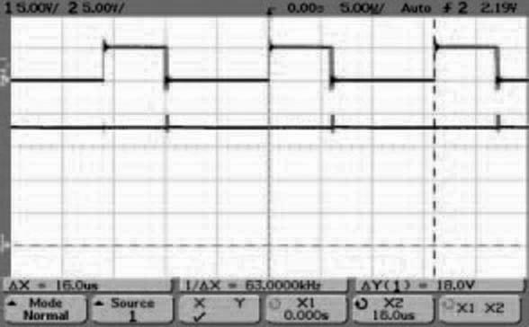
Figure 4 and Figure 5 are oscilloscope photos from a working example of the boost converter implementing the basic topology in Figure 1 and the control block in Figure 3. The peak current in the inductor is 0.3 mV × 0.2 Ω = 1.5 A (Figure 4). The on-time is approximately 5.9 µsec. The output voltage is 18 V into a 72 Ω load (Figure 5). The efficiency is approximately 90%. These boost-converter design and control ideas are just a few of the many possible ones using a PIC16C782 device.
 |
|
| Figure 5. | The example shows the duty cycle (top) and the output voltage (bottom) of the circuit in Figure 1. |