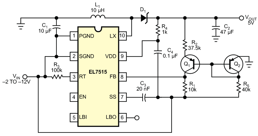
Assume that a design requires positive voltage, but only a negative-voltage power source is available. Using a standard boost-converter IC in the circuit of Figure 1, you can efficiently generate a positive voltage from a negative source. The boost converter generates an output voltage that’s higher than the input voltage. Because the output voltage – 5 V in this example – is higher than the negative-input-voltage ground level, the circuit does not violate the boost-converter principle.
 |
|
| Figure 1. | By using its ground terminals as the negative-voltage input, a boost converter can efficiently generate a positive output voltage. |
The circuit in Figure 1 uses the EL7515, a standard boost converter. The ground pins of the converter IC connect to a negative-voltage input source. Ground becomes the “positive” input source. VOUT is as follows:
The Q1 and Q2 pnp transistors form a translator that scales the 5 V output voltage (referred to ground) to a feedback voltage referred to the negative input. The transistor pair also eliminates temperature-change and voltage-drop effects. As the negative input voltage decreases, Q2 runs at an increasingly higher current than Q1, causing additional transistor-offset mismatch.
 |
|
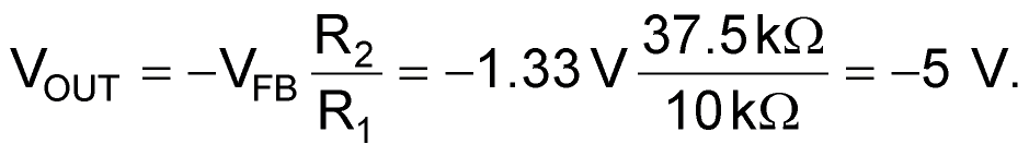
| Figure 2. | The line regulation is within ±40 mV over the full range of negative inputs. |
For optimal line regulation, you should set Q1 and Q2 to operate at the same currents with the nominal input-voltage applied. Figure 2 shows the line-regulation results. The maximum output-to-input voltage difference must be within the boost converter’s internal power FET drain-to-source breakdown voltage (VDS).
 |
|
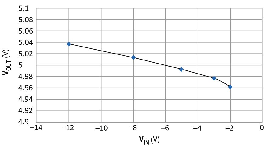
| Figure 3. | The output voltage varies by less than 14 mV over the full range of output currents. |
For the EL7515, the maximum VDS is 18 V. For the 5 V output, the minimum (most negative) input voltage is –12 V. A 1 V safety margin compensates for the D1 diode drop and any voltage spikes on the drain of the power FET. Figure 3 shows the load-regulation test results.
 |
|
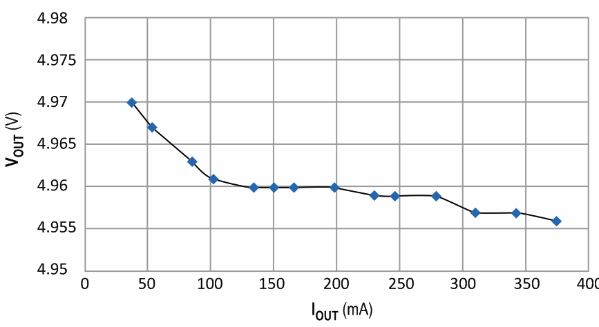
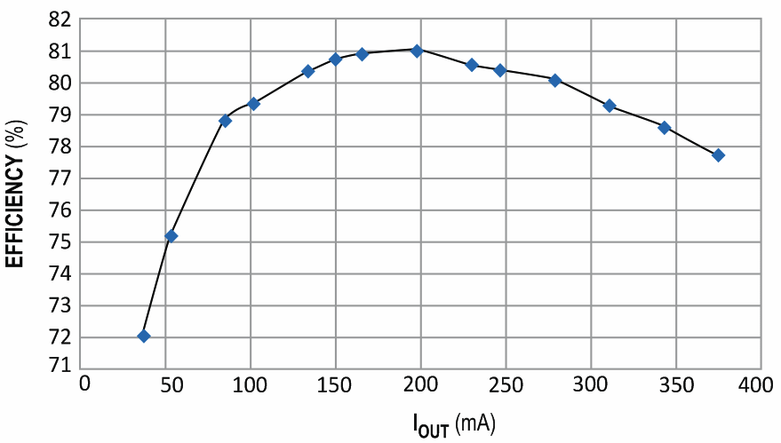
| Figure 4. | The efficiency of the circuit peaks at 81% for medium output current (200 mA). |
The maximum output current is a function of the input-to-output voltage ratio and current- limit setting of the boost converter. As Figure 4 shows, the circuit yields greater than 80% efficiency at 200-mA output.