Many power-supply designs rely on accurately sensing the voltage across a current-sense element. Multiphase regulators use the sense voltage to force current sharing among phases, and single-phase regulators to control the current-limit setpoint. As internal complexity and clock speeds increase, processors impose narrower operating margins for power-supply voltages and currents, which in turn make accurate current sensing critically important. The most accurate of several available methods involves inserting a low-value current-sensing resistor in the power supply's output path. Another popular technique uses the parasitic resistance of a switching regulator's output inductor as the sense element. For either method, currents of 20 A or more per power-supply phase impose a sense-resistance limit of approximately 1 mΩ. Precision resistors of 1% accuracy are available at reasonable cost, but an error of 1% of 1 mΩ amounts to only 10 µΩ.
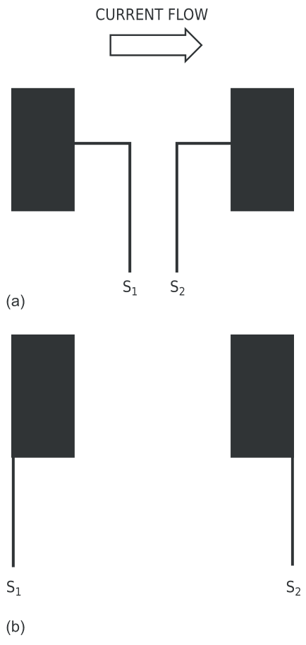
The resistance of solder joints that attach a sense resistor or inductor can easily exceed 10 µΩ and, worse yet, can vary significantly during a production run. In the past, discrete four-wire resistors provided separate high-current and sense-voltage connections, allowing accurate Kelvin sensing and excluding voltage drops that the high-current connections introduce. Unfortunately, four-wire sense resistors or inductors are unavailable in low cost SMD packages. Thus, most power-supply designers use two-wire sense components and apply a Kelvin-connection pc-board-layout technique (Figure 1). However, test results reveal that applying conventional Kelvin sensing techniques to low-value resistors introduces transduction errors as high as 25% – an unacceptable error margin for designs that require high accuracy.
 |
|
| Figure 1. | Conventional solder pads offer two choices for Kelvin connections: on the pads’ inner edges (a) or outer corners (b). |
So, what's a power-supply designer to do? The answer involves a slight variation on an old idea that requires only a minor change in a sense resistor's mounting footprint. To compare performance of conventional Kelvin connections versus the proposed method, a test board includes three pc-layout footprints for installation of 1-mΩ, 1%-accurate, surface-mount resistors. In all three patterns, current enters and exits the resistor via traces (not shown) on the pads' left and right sides, respectively.
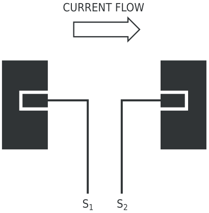
In Figure 1a, applying a current of 4.004 A produces a sense voltage at the Kelvin terminals of 4.058 mV, a 1.35% error. At 8.002 A, the sense voltage at the Kelvin terminals measures 8.090 mV, a 1.1% error. In Figure 1b, a current of 4.004 A produces a sense voltage at the Kelvin terminals of 5.01 mV, a 25% error. At 8.002 A, the sense voltage at the Kelvin terminals measures 9.462 mV for an error of 18.2%. Figure 2 shows an improved component footprint. Each large solder pad includes a central cutout area that partially surrounds a narrow pad that solders directly to the sense element and thus carries no current. This approach removes from the sense path the large-area solder joints that mount the part and carry high load current.
 |
|
| Figure 2. | Modified pads provide isolated Kelvin connections that eliminate errors introduced by voltage drops across soldered connections carrying high current. |
When you apply a current of 4.002 A to the pads in Figure 2, voltage at the Kelvin terminals measures 4.004 mV, a 0.05% error. At 8.003 A, the sense voltage measures 8.012 mV, an error of only 0.11% and an order of magnitude improvement over Figure 1a. Sense-voltage variation over temperature should greatly improve, and solder-thickness variation no longer affects the sense voltage. Best of all, the technique costs nothing to implement.
Obviously, the technique in Figure 2 works only with terminations sufficiently wide to allow dividing the solder pad into three sections and still retain adequate soldering area to handle the highcurrent connections. However, for many designs, this simple technique can significantly improve the accuracy of current sharing, V-I load-line characterization, and current-limit setpoints.