Abstract
This article details a method of generating dual-output voltage rails that provide both the positive and negative rails for a device power supply (DPS) while requiring only one bidirectional power supply. The traditional method of powering device power supplies uses two bidirectional (sourcing and sinking current capability) power supplies, one for the positive rail and one for the negative rail. This setup is bulky and costly.
Introduction
A DPS is used with automatic test equipment (ATE) and other measurement devices. ATEs are computerized machinery that automates traditional manual electronic test equipment to evaluate functionality, quality, performance, and stress tests.
These ATEs require a four-quadrant operation for their DPS. A DPS is a four-quadrant power supply that can source and sink current while having positive or negative voltage. To use the DPS for higher current applications, the solution will gang up multiple DPS devices to increase their current capability. Since the DPS can both sink and source current, the power supply for the DPS must have the same capability. The dual-output voltage rail is developed to reduce the number of bidirectional supplies needed to one, while still providing positive and negative bidirectional capable sources for the DPS. Making a bidirectional positive supply is straightforward as there are many available integrated circuits (ICs) that can source and sink current. The problem is that the negative supply needs to source and sink current as well, as required by the device under test (DUT). One solution is to use a bidirectionally capable buck IC that can be configured to function as an inverting buck-boost converter. One example is the LTC3871, which can be used for both the positive and negative rails, as it is a bidirectional buck or boost controller.
Designing an inverting buck-boost converter using a buck IC
 |
|
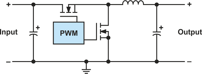
| Figure 1. | A buck converter. |
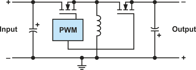
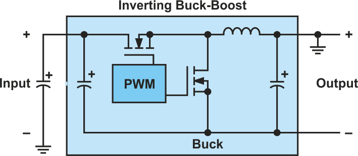
Figure 1 shows a simplified schematic diagram of a buck converter. It takes a positive input and outputs a positive output with a lower magnitude. Figure 2 shows an inverting buck-boost converter that takes a positive input and outputs a lower or higher negative magnitude. As seen in Figure 3, a buck topology can be converted to an inverting buck-boost topology by doing the following:
- Converting the positive output of the buck converter to the system ground
- Converting the system ground of the buck converter as the negative output node
- Applying input voltage between the VIN and positive output of the buck converter
 |
|
| Figure 2. | An inverting buck-boost converter. |
 |
|
| Figure 3. | Converting a buck converter to an inverting buck-boost configuration. |
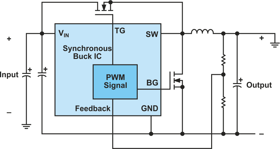
Figure 4 shows a simplified schematic on how to convert a buck IC to an inverting buck-boost configuration.
 |
|
| Figure 4. | A buck IC used in an inverting buck-boost topology. |
How a converted buck IC works
Sourcing current
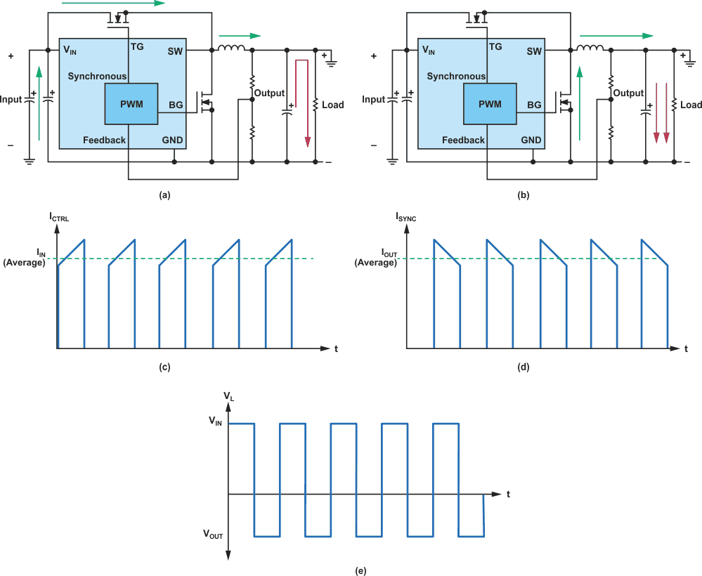
Figure 5 shows the waveforms for an inverting buck-boost converter and the current flow when sourcing current. Figure 5a shows the current flow throughout the converter when the control MOSFET is turned on. Figure 5c shows the current flowing through the control MOSFET and its average is the input current. During this time, the inductor starts storing energy, ramping up the current while the output capacitor supplies the load. The inductor voltage is equal to the input voltage in this period.
When the control MOSFET is turned off, the sync MOSFET is turned on, and Figure 5b shows the current flow through it. The output current is the average current of the sync MOSFET, and the inductor voltage is equal to the output voltage. As the inductor supplies the load and capacitor, its current starts to go down. This will repeat every switching cycle.
 |
|
| Figure 5. | (a) Current flow during on-time, (b) current flow during off-time, (c) the current through the top/control MOSFET (ICTR), (d) the current through the bot/sync MOSFET (ISYNC), and (e) inductor voltage. |
The feedback of the converter controls the pulse-width modulation (PWM) to regulate the output voltage to the desired level, which is set by the voltage divider resistors. Equation 1 shows the relationship between the output voltage and input voltage.
 |
(1) |
where
VOUT – output voltage,
VIN – input voltage,
D – duty cycle,
η – efficiency of the system.
The output voltage is greater than the input voltage when the duty cycle is greater than 50% and less than the input voltage when the duty cycle is less than 50%.
Sinking current
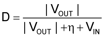
When the converter starts sinking current, the current flows from the output to the input as denoted in figures 6a and 6b. The current flowing through the control and sync MOSFETs are in figures 6c and 6d, respectively. Since the converter is sinking current, a negative current is seen flowing through the MOSFETs. The Test Result section shows the negative inductor current during the sinking.
 |
|
| Figure 6. | (a) Current flow during on-time, (b) current flow during off-time, (c) current through the top/control MOSFET (ICTR), and (d) current through the bot/sync MOSFET(ISYNC). |
Test result
 |
|
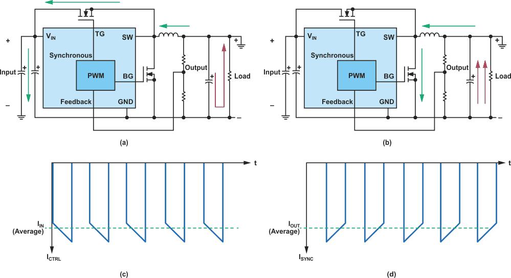
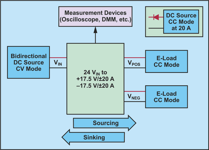
| Figure 7. | A board setup for source-sink testing. |
Figure 7 shows the actual test setup to test the source-sink and sink-source capability of the design. Figure 8 shows the block diagram of the setup. The bidirectional DC source acts as the supply of the VPOS and is in CV mode. The other DC source is connected to the output of the VNEG. This DC source controls the amount of current that is sunk into the system. A blocking diode is connected in series with this DC source to ensure that no current will flow into it when the converter is sourcing current. The e-load is used as the initial load to show that the system is capable of transitioning from sourcing to sinking and vice versa.
 |
|
| Figure 8. | A block diagram for the setup. |
 |
|
| Figure 9. | A VNEG source to sink transition (+1 A to –20 A). |
The waveforms captured are shown in Figure 9. When the DC supply is turned on, the VNEG rail starts to sink current. As seen in the inductor current waveform, it transitions from positive current to negative current. When the VNEG is sinking current, the system is open loop during this condition and the source-sink current is controlled by the CC mode of the external DC source. This is also true for the VPOS in Figure 10. When the DC source connected to its output is turned on, the VPOS rail starts to sink current.
 |
|
| Figure 10. | A VPOS source to sink transition (+1 A to –20 A). |
 |
|
| Figure 11. | A VNEG sink to source transition (–20 A to +1 A). |
The waveforms captured and shown in Figure 11 are the source to sink transition behavior of the system. As seen in the inductor current, it transitions from negative current to positive current. This indicates the transition back to sourcing current when the injected DC voltage across the VNEG is removed. This is also true for the VPOS rail shown in Figure 12.
 |
|
| Figure 12. | A VPOS sink to source transition (–20 A to +1 A). |
Conclusion
The dual-output voltage rail reduces the equipment needed as it is already bidirectional capable on both the VPOS and VNEG. It is also more efficient as the current sunk on one rail is used to power the other rail, reducing the current that is sourced by the main supply. An additional benefit of the converter is that it allows for a greater selection of ICs to choose from when designing a bidirectional inverting buck-boost converter.
References
- Kessler, Matthew. “AN-1083 (Rev. A): Designing an Inverting Buck Boost Using the ADP2300 and ADP2301 Switching Regulators.” Analog Devices, Inc., 2010.
- Yang, Ricky. “AN-1168 (Rev. 0): Designing an Inverting Power Supply Using the ADP2384/ADP2386 Synchronous Step-Down DC-to-DC Regulators.” Analog Devices, Inc., 2012.