Back on December 3, 2024, a Design Idea (DI) was published, “Single-supply single-ended inputs to pseudo class A/B differential output amp” (Ref. 1), which created some discussion about using the circuit as a full wave rectifier.
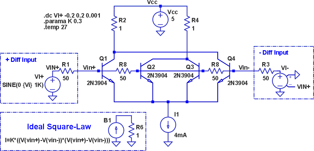
The circuit shown in Figure 1 is an LTspice implementation built around a bipolar differential amplifier with Q1 and Q3 serving as the + and – active differential input devices, respectively.
 |
|
| Figure 1. | An LTspice implementation built around a bipolar differential amplifier with Q1 and Q3 serving as the + and – active differential input devices, respectively, allowing the circuit to be better suited for square-law functions. |
Additional devices Q2 and Q4 are added at the “center point” between Q1 and Q3, and act such that the collector currents of all devices are equal when no differential voltage is present.
This occurs because resistors R7 and R8 create a virtual differential zero-volt “center point” between the + and – differential inputs, and all device VBE’s are the same, neglecting the small voltage drop across R7 and R8 due to Q2 and Q4 base bias currents.
R7 and R8 set the differential input impedance for the circuit configuration, where R1 and R3 set the signal source differential impedances for the simulations.
The device emitter currents are controlled by the “tail current source” I1 at 4 mA; thus, each device has an emitter current of ~1 mA with zero differential input. Note the -Diff Input signal is created by using a voltage-controlled voltage source with an effective gain of –1 due to the inverted sensing of the +Diff Input voltage (VIN+). This arrangement allows the input signal to be fully differential when LTspice controls the VI+ voltage source during signal sweeps.
This is not part of the circuit but used for comparisons: Voltage-controlled current source, B1, is configured to produce an ideal square-law characteristic by squaring the differential voltage (Vin+ – Vin–) and scaling by factor “K”.
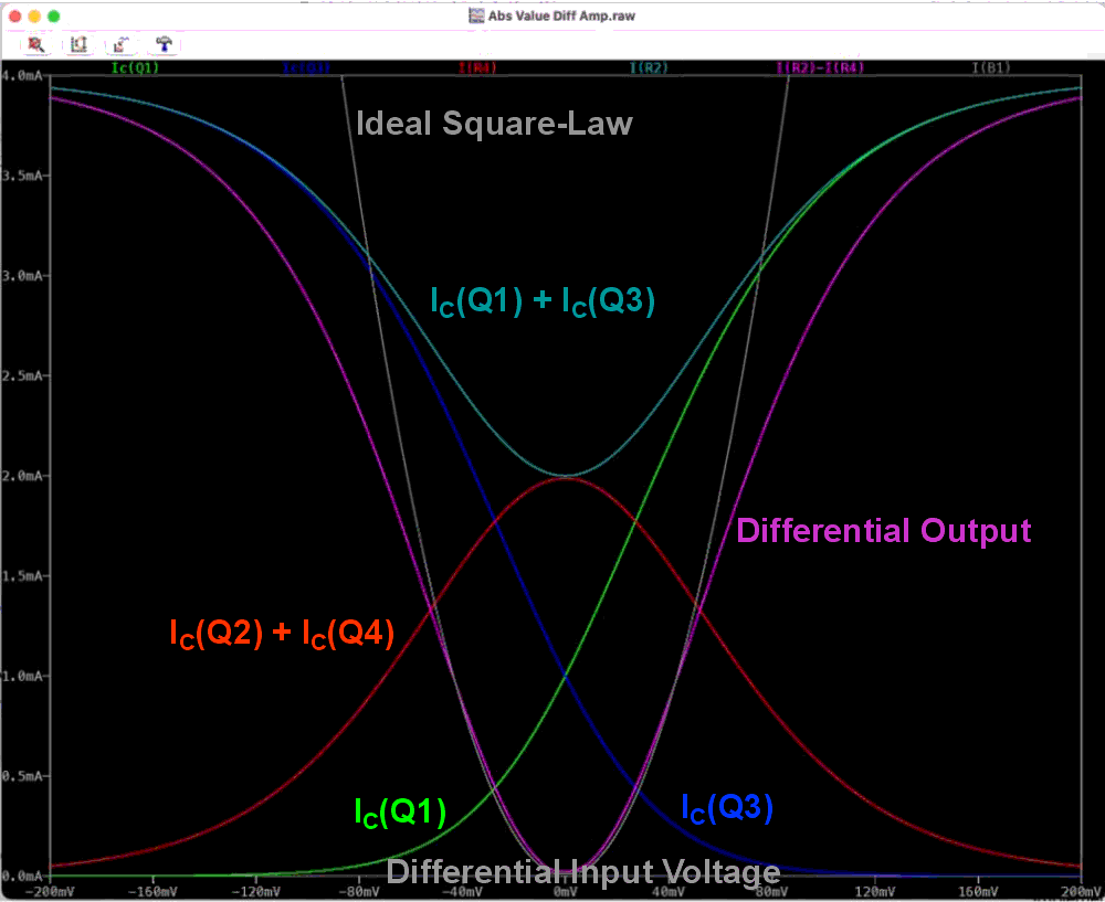
Figure 2 shows the simulation results of sweeping the differential input voltage sources from –200 mV to +200 mV while monitoring the various device currents. Note the differential output current, which is:
[IC(Q1) + IC(Q3)] – [IC(Q2) + IC(Q4)]
closely approximates the ideal square-law with a scale factor of 0.3 (amps/volt) for differential input voltages of ±60 mV.
 |
|
| Figure 2. | Simulation results of sweeping the differential input voltage sources from 200 mV to +200 mV while monitoring the various device currents. |
Please note this circuit is a transconductor type where the output is a differential current controlled by a differential input voltage.