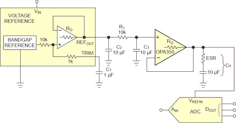
High-resolution mixed-signal devices present an interesting challenge as you try to find the right voltage-reference design. Although no universal approach exists for these voltage-reference designs, the circuit in Figure 1 presents an interesting approach for greater-than-15-bit converters.
 |
|
| Figure 1. | Although no universal approach exists for these voltage-reference designs, this circuit presents an interesting approach for converters with greater than 15 bits of resolution. |
Some design issues of concern with high-resolution converters are voltage-reference noise, stability, and the reference circuit’s ability to drive the voltage-reference pin of your converter. The passive filter comprising R1, C2, and C3 dramatically reduces the voltage-reference noise. The corner frequency of this lowpass filters 1.59 Hz. This filter reduces both broadband and extremely low-frequency noise. The additional RC filter brings the noise level under control enough for a 20-bit ADC. This situation is encouraging. However, if current is pulled through R1 from the ADC’s reference pin, the voltage drop will corrupt the conversion by introducing a voltage drop with each bit decision (Reference 1).
The circuit diagram in Figure 1 has an operational amplifier to isolate the lowpass filter comprising R1, C2, and C3 and to provide adequate drive to the ADC’s reference pin. The input bias current of the OPA350 CMOS op amp is 10 pA at 25 °C. This current combines with R1’s resistance of 10 kΩ to generate a constant 100-nV dc drop. This level of voltage drop does not change a 23-bit ADC’s final bit decision. The input bias current of the op amp changes over temperature, but you can expect a maximum current that is no more than 10 nA at 125 °C, generating a change of 100 μV over a 100 °C temperature range.
It is useful to put this voltage drop across R1 into perspective. This voltage drop adds to the errors of the voltage-reference device. Suppose that the initial error of the voltage-reference circuit is ±0.05% with an error over temperature of 3 ppm/°C. With a reference of 4.096 V, the initial voltage-reference error is equal to 2.05 mV at room temperature plus 1.23 mV at 125 °C. In the circuit in Figure 1, the voltage-reference device dominates over the op amp’s offset and input bias-current errors. An ADC that connects to the circuit in Figure 1 sees the summation of the errors from the voltage reference, R1, and OPA350 as a gain error.
The op amp drives a 10-μF capacitor, C4, and the ADC’s voltage-reference input pin. The charge residing on C4 provides the needed charge during the ADC’s conversion. During the ADC’s acquisition and conversion, the size of C4 provides a stiff voltage reference for the ADC’s reference pin, which usually has an input capacitance of approximately 2 to 50 pF.
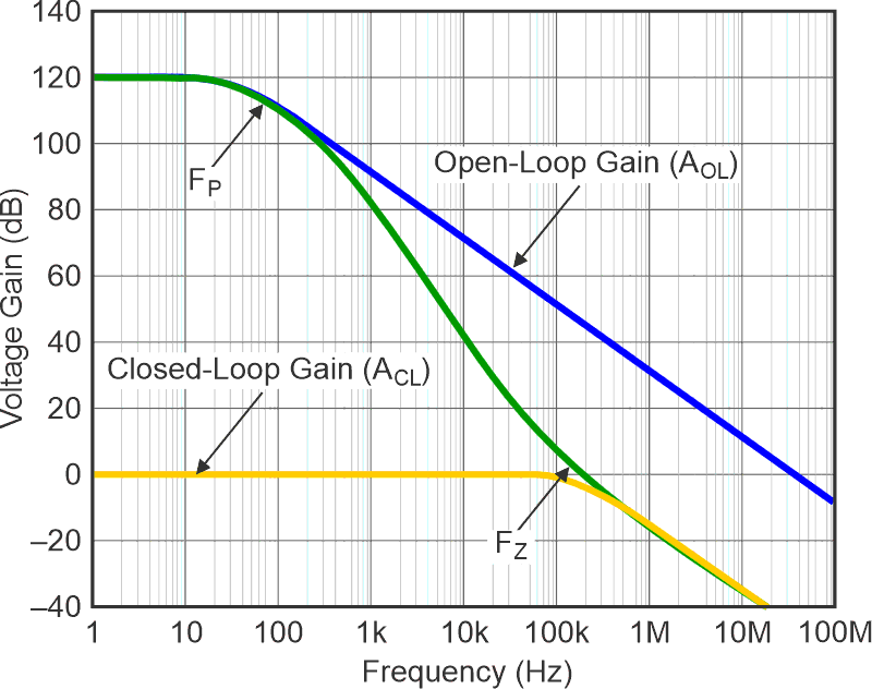 |
|
| Figure 2. | A circuit with good stability is one in which the modified op amp's open-loop-gain curve and the closed-loop voltage-gain curve's rate of closure is 20 dB. |
You can compromise the amplifier’s stability because C4 and the op amp’s open-loop output resistance, RO, modify the amplifier’s open-loop-gain curve. Basically, a circuit with good stability is one in which the modified op amp’s open-loop-gain curve and the closed loop voltage-gain curve’s rate of closure is 20 dB (Figure 2). In this stable circuit, the following equations calculate the frequency locations of the pole and zero:
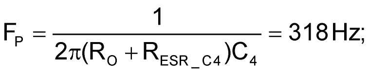
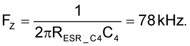
The open-loop output resistance of the OPA350 is 50 Ω, and the ESR (equivalent series resistance) of C4 is 2 mΩ.
References
- Baker, Bonnie, "Taking the mixed-signal voltage reference to a higher level."
- Baker, Bonnie, "Just use a 100Ω resistor: Understanding a rule of thumb for oscillating amplifiers."