In the control of nonlinear and linear systems, sometimes a slight nonlinearity is intentionally inserted into the closed control loop. “Slight” here means that the output of the inserted element starts to vary linearly, but only once the input exceeds a nonzero threshold value. For inputs from zero to the threshold, the output of the element has zero value. The result is that adding of this nonlinear element can quench damped oscillations, which are typical for feedback systems.
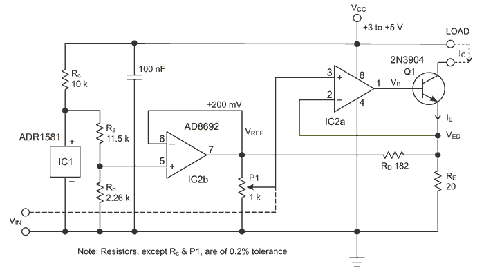
The unipolar voltage-to-current converter in Fig. 1 is based on a classical connection of op-amp IC2a and NPN transistor Q1. The regulated current flows through emitter resistor RE, which acts here as a simple passive current-to-voltage converter. In the closed-loop, actual negative feedback is the voltage fed to the inverting input of IC2a. A dead-band in the V-I characteristic is created by current flowing from the source of reference voltage, VREF, through resistors RD, RE to ground. The reference voltage VREF is derived from the band-gap cell IC1, resistive divider Ra, Rb, and op amp IC2b.
 |
|
| Figure 1. | Output current of the converter rises linearly for input voltage rising within the range of 20 mV to 200 mV, while it has zero value for VIN below 20 mV. |
To evaluate this dead-band quantitatively, you can firstly assume VIN equal to zero. The op-amp tries to force VED to zero as well. This however is not possible, as the B-E junction of Q1 acts now as a reverse-biased diode. The result is that the emitter current of Q1 is zero, and consequently the voltage-drop at resistor RE, is:
As the same voltage appears at inverting input of the op amp, its output is saturated at zero-level.
When you start to elevate the level of VIN from zero value, the situation remains steady until VIN value exceeds that of VED, given by Equation 1. At that instant the output voltage of op-amp IC2a becomes positive, causing a current to flow through the emitter of Q1. The higher the value of VIN is, the higher is the emitter current of Q1. Due to a strong negative feedback, the dependence IC(VIN) is linear for VIN within the VED to VREF range. To evaluate the output current at full-scale input voltage, VIN = VREF, you can realize that the RD resistor has the same voltage, VREF, at both its ends, so no current flows through it. The equivalent emitter resistor at the full-scale output current is therefore RE itself, and the value of emitter full-scale current is VREF/ RE.
The output current flowing across the collector of Q1 and positive supply terminal, is very close to emitter current:
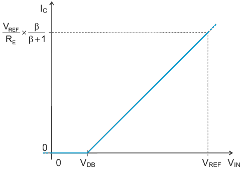
where β is the current gain of Q1. The V-I characteristic of the converter is drawn in Fig. 2.
 |
|
| Figure 2. | |
For the 2N3904 transistor, β ≈ 230; thus the collector current is about 0.44% lower than its emitter current. To lower this error, you could use a Darlington pair, or a cascade of two bipolar transistors, in place of. The input voltage, VIN, can be derived either from potentiometer P1 or an external source.
If you choose, for example VDB = 0.1×VREF, VDB = VED you get from Equation 1 that RD = 9RE. A theoretical dependence of output current on input voltage is depicted in Fig. 2.
Experimentally, VREF = 0.19645 V and full-scale emitter voltage VED = 0.19660 V have been measured. The VDB has been determined by detecting an abrupt change at the output of IC2a of either zero-to-positive, or positive-to-zero voltage transitions, and by measuring the VIN value at this instant. VDB = 19.75 mV for positive transitions and VDB = 19.70 mV for negative transition have been measured.