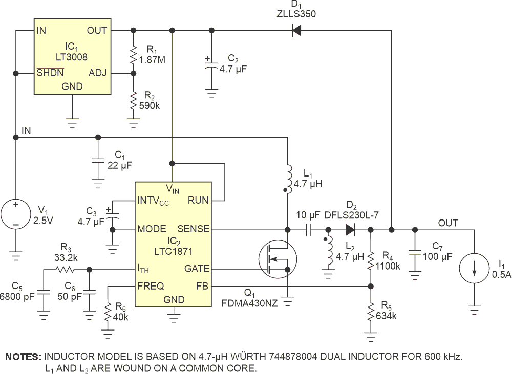
The switching power supply in Figure 1 produces 3.3 V dc from an input voltage of 2.5 to 20 V dc with high efficiency. The circuit operates at an input voltage as low as 1.5 V once it starts from a minimum of 2.5 V dc, allowing the switcher to fully discharge a pair of alkaline cell batteries nearing end of life. The power supply can also run efficiently off higher input voltages, such as 12 V automotive power. The heart of the circuit is a SEPIC (single-ended-primary-inductance-converter)-based switching power supply, which provides an output voltage greater than or less than the input voltage (Reference 1).
 |
|
| Figure 1 | The power supply can provide a 3.3 V output from 2.5 to 20 V input voltages. It needs 2.5 V to start. |
This power supply includes bootstrap circuitry comprising IC1, an LT3008 voltage regulator; Schottky diode D1; and capacitor C2. It needs a minimum of 2.5 V to start. Voltage regulator IC1 provides 2.5 V to start SEPIC controller IC2. Once the output voltage of the SEPIC power supply reaches its normal output voltage of 3.3 V, D1 lets the output power of the switcher flow back to power IC2. Once this action occurs, IC1 drops out of the circuit because the voltage at its output is above its setpoint voltage. The converter’s own output now powers IC2, and the regulator’s internal circuitry prevents backflow of power through IC1. MOSFET Q1 has low threshold voltage, appropriate on-resistance to provide current feedback to IC2, and a maximum drain-to-source voltage of 30 V to allow for operation up to a 20 V input.
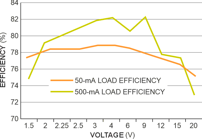
The bootstrap circuit allows the converter to run from very low input voltages by maintaining the input voltage to IC2, and it increases efficiency at high input voltages by eliminating the use of IC2’s internal linear voltage regulator. Figure 2 shows the efficiency of the prototype power supply at both 50- and 500-mA loads. The power supply’s efficiency is consistent over a range of operating voltages because of the bootstrapping circuit.
 |
|
| Figure 2 | The power supply’s efficiency is consistent over 50- and 500-mA loads. |
Because the circuit uses a low-threshold- voltage MOSFET, the switch, keeping the gate drive voltage low, reduces the total charge that must go into and out of the MOSFET gate, further improving efficiency. SEPIC controller IC2 normally uses its internal low-dropout capability to generate an operating voltage of 5 V from the input. Running IC2 from the bootstrapped output reduces IC2’s operating voltage to approximately 3 V, which also limits the drive voltage to Q1’s gate.
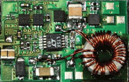
The PCB (printed-circuit-board) design and the choice of coupled inductors for this power supply are critical for good performance. For the power supply to achieve high efficiency at low input voltages and high output current, the coupled inductor must have low-resistance windings, and the high current tracks should use wide copper pours to minimize resistance losses and unwanted inductance.
A prototype of the power supply measures 23 × 15 × 3.5 mm (Figure 3). It uses a custom coupled inductor, but you can choose from many off-the-shelf coupled inductors available from BH Electronics, Coilcraft, and WЬrth Elektronik.
 |
|
| Figure 3 | The complete power supply fits onto a 23×15×3.5-mm PCB. |
Reference
- “Designing a SEPIC Converter,” Application Note 1484.