Marty Merchant, Linear Technology
Design Note 507
Introduction
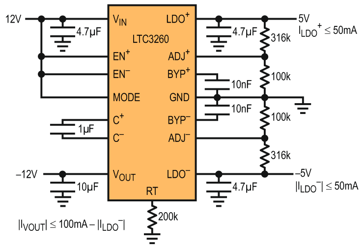
Dual-polarity supplies are commonly needed to operate electronics such as op amps, drivers, or sensors, but there is rarely a dual-polarity supply available at the point of load. The LTC3260 is an inverting charge pump (inductorless) DC/DC converter with dual low noise LDO regulators that can produce positive and negative supplies from a single wide input (4.5 V to 32 V) power source. It can switch between high efficiency Burst Mode® operation and low noise constant frequency mode, making it attractive for both portable and noise-sensitive applications. The LTC3260 is available in a low profile 3 mm × 4 mm DFN or a thermally enhanced 16-lead MSOP, yielding compact solutions with minimal external components. Figure 1 shows a typical 12 V to ±5 V application featuring the LTC3260.
 |
|
| Figure 1. | Typical 12 V to ±5 V Supply. |
Inverting Charge Pump
The LTC3260 can supply up to 100 mA from the inverted input voltage at its charge pump output, VOUT. VOUT also serves as the input supply to a negative LDO regulator, LDO–. The charge pump frequency can be adjusted between 50 kHz to 500 kHz by a single external resistor. The MODE pin is used to select between a high efficiency Burst Mode operation or constant frequency mode to satisfy low noise requirements.
Constant Frequency Mode
A single resistor at the RT pin sets the constant operating frequency of the charge pump. If the RT pin is grounded, the charge pump operates at 500 kHz, where the open-loop output resistance (ROL) and the output ripple are optimized, allowing maximum available output power with only a few millivolts peak-to-peak output ripple.
 |
|
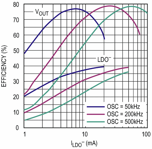
| Figure 2. | LTC3260 VIN to VOUT and VIN to LDO– Efficiency vs Frequency for the Circuit in Figure 1. |
Light load efficiency can be increased by reducing the operating frequency, as shown in Figure 2, but at the expense of increased output ripple. The lower operating frequency produces a higher effective open-loop resistance (ROL), but the reduced switching rate also reduces the input current, resulting in increased efficiency at light loads. Furthermore, at relatively heavy loads, the increased ROL reduces the effective difference between VOUT and LDO– – decreasing the power dissipation in the negative LDO. The cumulative result is higher overall efficiency with high input voltages and/or light loads.
 |
|
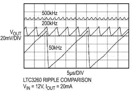
| Figure 3. | VOUT Constant Frequency Ripple Comparison at 500 kHz, 200 kHz and 50 kHz at 20 mA Load. |
Reducing the frequency increases the output ripple as shown by the expression below and in Figure 3.
where
In general, constant frequency mode is suitable for applications requiring low output ripple even at light loads, but further gains in light load efficiency can be gained by using Burst Mode operation, described below.
Burst Mode Operation
 |
|
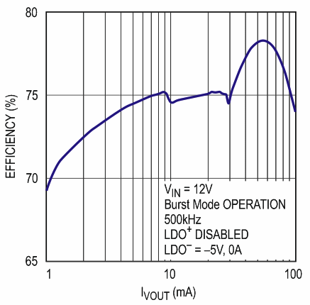
| Figure 4. | LTC3260 Burst Mode Operation Efficiency. |
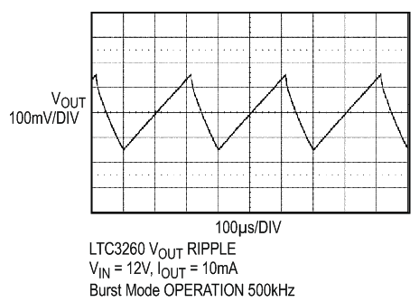
Figure 4 shows the light-load efficiency of the charge pump in Burst Mode operation. Burst Mode operation increases the output ripple over constant frequency mode, but the increase in ripple is only a small percentage of VIN, as shown in Figure 5.
 |
|
| Figure 5. | VOUT Ripple in Burst Mode Operation. |
Burst Mode operation is implemented by charging VOUT close to –VIN. The LTC3260 then enters a low quiescent current sleep state, about 100 μA with both LDO regulators enabled, until the burst hysteresis is reached. Then the charge pump wakes up and the cycle repeats. The average VOUT is approximately –0.94VIN. As the load increases, the charge pump runs more often to keep the output in regulation. If the load increases enough, the charge pump automatically switches to constant frequency mode in order to maintain regulation.
Dual LDOs
Both of the LTC3260’s LDOs – the positive LDO regulator supplied from VIN, and the negative LDO regulator supplied from VOUT – are capable of supporting 50 mA loads. Each LDO has a dropout voltage of 300 mV with a 50 mA output and has an adjust pin, allowing the output voltage to be set by a simple resistor divider. The LDO regulators can be individually enabled. The EN– pin enables both the inverting charge pump and LDO–. When both regulators are disabled, the part shuts down with only 2 μA of quiescent current. The LDO references can be filtered by adding a capacitor on each of the bypass pins to further reduce noise at the LDO regulator outputs.
Conclusion
The LTC3260 produces low noise positive and negative supplies from a single positive power source. The LTC3260 features optional Burst Mode operation for light-load efficiency in battery-powered devices, or low noise constant frequency mode for noise-sensitive applications. The LTC3260’s combination of inverting charge pump and dual LDO regulators yields elegant solutions to applications with 4.5 V to 32 V inputs.
Appendix
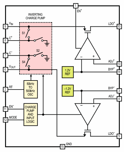
The LTC3260 Block Diagram