Analog Devices
Circuit Note CN0191
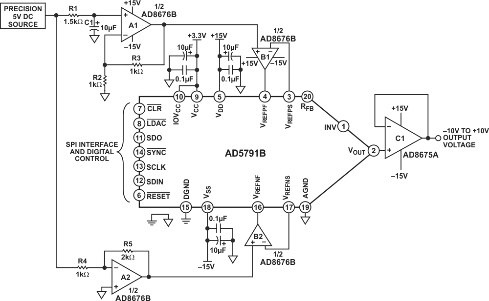
Circuit Function and Benefits
The circuit shown in Figure 1 provides a programmable 20-bit voltage with an output range −10 V to +10 V, ±1 LSB integral nonlinearity, ±1 LSB differential nonlinearity, and low noise.
The digital input to the circuit is serial and is compatible with standard SPI, QSPI™, MICROWIRE®, and DSP interface standards. For high accuracy applications, the circuit offers high precision, as well as low noise, and this is ensured by the combination of the AD5791, AD8675, and AD8676 precision components.
 |
|
| Figure 1. | 20-Bit Accurate, ±10 V Voltage Source (Simplified Schematic: All Connections and Decoupling Not Shown) |
The reference buffer is critical to the design because the input impedance at the DAC reference input is heavily code dependent and will lead to linearity errors if the DAC reference is not adequately buffered. With a high open-loop gain of 120 dB, the AD8676 has been proven and tested to meet the settling time, offset voltage, and low impedance drive capability required by this circuit application. The AD5791 is characterized and factory calibrated using the AD8676 dual op amp to buffer its voltage reference inputs, further enhancing confidence in partnering the components.
This combination of parts provides industry-leading 20-bit integral nonlinearity (INL) of ±1 LSB and differential nonlinearity (DNL) of ±1 LSB, with guaranteed monotonicity, as well as low power, small PCB area, and cost effectiveness.
Circuit Description
The digital-to-analog converter (DAC) shown in Figure 1 is the AD5791, a high voltage, 20-bit converter with SPI interface, offering ±1 LSB INL and ±1 LSB DNL performance and 7.5 nV/√Hz noise spectral density. The AD5791 also exhibits an extremely low temperature drift of 0.05 ppm/°C. The precision architecture of the AD5791 requires force-sense buffering of its voltage reference inputs to ensure specified linearity. The amplifiers (B1 and B2) chosen to buffer the reference inputs should have low noise, low temperature drift, and low input bias currents. The recommended amplifier for this function is the AD8676, an ultraprecision, 36 V, 2.8 nV/√Hz, dual op amp exhibiting low offset drift of 0.6 μV/°C and input bias currents of 2 nA.
Figure 1 shows the AD5791 configured with independent positive and negative reference voltages, such that the output voltage ranges from the negative reference voltage to the positive reference voltage, in this case from −10 V to +10 V. The output buffer is the AD8675, a single op amp version of the AD8676, used for its low noise and low drift. The AD8676 amplifier (A1 and A2) is also used to scale the +5 V reference voltage to +10 V and −10 V. R2, R3, R4, and R5 in these scaling circuits are precision metal foil resistors with 0.01% tolerance and a temperature coefficient of resistance of 0.6 ppm/°C. For optimum performance over temperature, resistor networks, such as the Vishay 300144 or VSR144 series can be used. The resistor values are selected to be low (1 kΩ and 2 kΩ) to keep noise in the system low. R1 and C1 form a low pass filter with a cutoff frequency of approximately 10 Hz. The purpose of this filter is to attenuate voltage reference noise.
Linearity Measurements
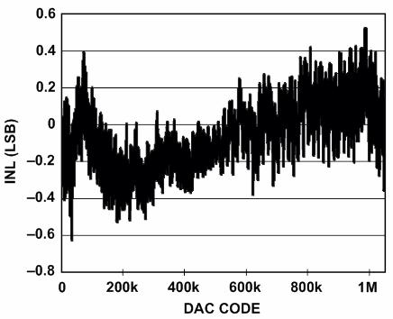
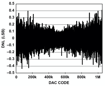
The following data demonstrates the precision performance of the circuit shown in Figure 1. Figure 2 and Figure 3 show integral nonlinearity and differential nonlinearity as a function of DAC code. As can be seen, both are significantly within the specifications of ±1 LSB and ±1 LSB, respectively.
 |
|
| Figure 2. | Integral Nonlinearity vs. DAC Code |
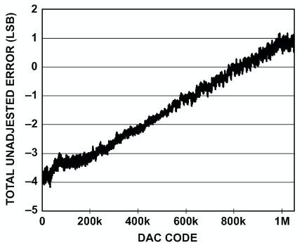
The total unadjusted error for the circuit consists of the dc errors combined together – that is, INL error, zero-scale error, and full-scale error. Figure 4 shows a plot of total unadjusted error as a function of DAC code. The maximum errors occur at DAC code zero (zero-scale error) and DAC code 1,048,575 (full-scale error). This is expected, and is due to the mismatches in resistor pair R2 and R3, resistor pair R4 and R5, and the offset errors of amplifiers A1, A2, B1, and B2 (see Figure 1).
 |
|
| Figure 3. | Differential Nonlinearity vs DAC Code |
The specified mismatch in the resistor pairs in this case is 0.02% maximum (the typical mismatch is far less than this). The amplifier offset errors are 75 μV maximum, or 0.000375% of full-scale range and are negligible relative to the error induced by the resistor mismatch. The maximum expected full-scale and zero-scale errors are, therefore, approximately 0.02%, or 210 LSBs each. Figure 4 shows the measured full-scale error to be 1 LSB and the measured zero-scale error to be 4 LSBs, or 0.0003% of full-scale range, indicating that all components are performing significantly better than their specified maximum tolerances.
 |
|
| Figure 4. | Total Unadjusted Error vs. DAC Code |
Noise Measurements
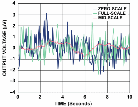
To be able to realize high precision, the peak-to-peak noise at the circuit output must be maintained below 1 LSB, which is 19.07 μV for 20-bit resolution and a 20 V peak-to-peak voltage range. Figure 5 shows peak-to-peak noise measured in the 0.1 Hz to 10 Hz bandwidth over a period of 10 seconds. The peak-to-peak values for each of the three conditions are 1.48 μV for mid-scale output, 4.66 μV for full-scale output, and 5.45 μV for zero-scale output. Mid-scale output exhibits the lowest noise, as it represents the noise from the DAC core only. The noise contribution from each voltage reference path is attenuated by the DAC when mid-scale code is selected.
 |
|
| Figure 5. | Voltage Noise in 0.1 Hz to 10 Hz Bandwidth |
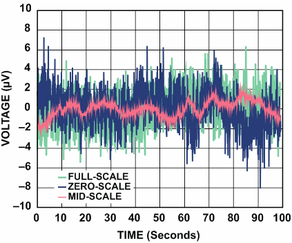
A real application, however, will not have a high-pass cutoff at 0.1 Hz to attenuate 1/f noise but will include frequencies down to dc in its pass band; therefore, the measured peak-to-peak noise will be more realistically as shown in Figure 6. In this case the noise at the output of the circuit was measured over a period of 100 seconds, effectively including frequencies as low as 0.01 Hz in the measurement. The upper frequency cutoff is at approximately 14 Hz and is limited by the measurement setup. For the three conditions shown in Figure 6 the peak-to-peak values are: 4.07 μV for mid-scale output, 11.85 μV for full-scale output, and 15.37 μV for zero-scale output. The worst case peak-to-peak value of 15.37 μV corresponds to approximately 0.8 LSB.
 |
|
| Figure 6. | Voltage Noise Measured Over 100 Second Period |
As the time period over which the measurement is taken is increased, lower frequencies will be included, and the peak-to-peak value will increase. At low frequencies, temperature drift and thermocouple effects become contributors to noise. These effects can be minimized by choosing components with low thermal coefficients, such as the AD5791, AD8675 and AD8676 and by giving careful consideration to circuit construction.
Common Variations
The AD5791 will support a wide variety of output ranges from 0 V to +5 V up to ±10 V, and values in between. The configuration as shown in Figure 1 can be used to generate symmetrical or asymmetrical ranges as required. Individual references are applied at VREFP and VREFN, and the output buffer should be configured for unity gain as described in the AD5791 datasheet, with the RBUF bit of the AD5791 internal control register set to a Logic 1.
The AD5791 also offers a gain of 2 mode of operation that generates a symmetrical bipolar output range from a single positive voltage reference as described in the AD5791 data sheet, removing the necessity to generate a negative voltage reference. This mode, however, will result in larger full-scale and zero-scale errors. This mode is selected by setting the RBUF bit of the AD5791 internal control register to a Logic 0.
Circuit Evaluation and Test
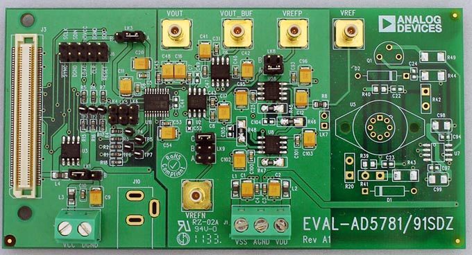
The circuit of Figure 1 was constructed on a modified AD5791 evaluation board (Figure 7). Details of the AD5791 evaluation board and test methods can be found in Evaluation Board User Guide, UG-185.
 |
|
| Figure 7. | Evaluation Board for the AD5791. |