A simple current source
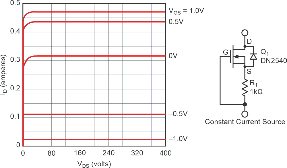
It has long been known that the simple combination of a depletion-mode MOSFET (and before these were available, a JFET) and a resistor made a simple, serviceable current source such as that seen on the right side of Figure 1.
 |
|
| Figure 1. | Current versus voltage characteristics of a DN2540 depletion mode MOSFET and the circuit of a simple current source made with one. |
This is evident from the figure’s left side, which shows the drain current versus drain voltage characteristics for various gate-source voltages of a DN2540 MOSFET. Once the drain voltage rises above a certain point, further increases cause only very slight rises in drain current (not visible on this scale). This simple circuit might suffice for many applications, except for the fact that the VGS required for a specific drain current will vary over temperature and production lots. Something else is needed to produce a drain current with any degree of precision.
Alternative current source circuits
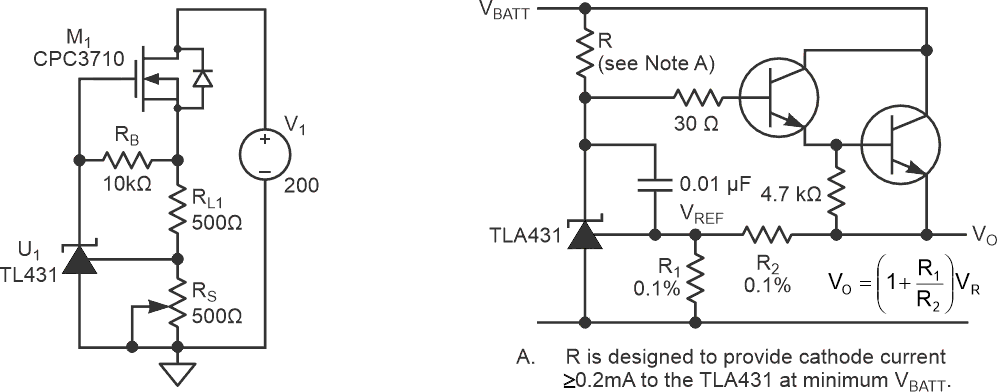
And so, we might turn to something like the circuits of Figure 2.
 |
|
| Figure 2. | A current source with a more predictable current, left (IXYS) and a voltage regulator which could be employed as a current source with a more predictable current, right (Texas Instruments). |
In these circuits, we see members of the ‘431 family regulating MOSFET source and BJT emitter voltages. The Texas Instruments circuit on the right demonstrates the need for an oscillation-prevention capacitor, and my experience has been that this is also needed with the IXYS circuit on the left.
Although RL1, RS, and R1 pass precise, well-regulated currents to the transistors in their respective circuits, resistors RB and R do not. RB’s current is subject to a not well-controlled VGS, and R’s is affected by whatever variations there might be in VBATT.
The MOSFET circuit is a true two-terminal current source, so a load can be connected in series with the current source at its positive or negative terminal. But then the load is always subjected to the poorly-controlled RB current.
The BJT is part of a three-terminal circuit, and for a load to avoid the VBATT-influenced current through R, it could only be connected between VBATT and the BJT collectors. Even so, variations in VBATT could produce currents, which lead to voltages that are not entirely rejected at the TLA431 cathode, and so would produce uncontrolled currents in the BJTs and therefore in the load.
A true two-terminal current source
Figure 3 addresses these limitations in circuit performance. In analyzing it, as always, I rely on datasheet maximum and minimum values whenever they are available, but resort to and state that I’m employing typical values when they are not.
 |
|
| Figure 3. | This circuit delivers predictable currents to U1 and M1 and therefore to a load. It’s a true two-terminal current source which accommodates load connection to both low and high side. |
U1 establishes
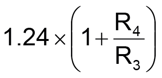
volts at VS and adds a current of
to the MOSFET drain.
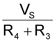
An additional drain current comes from:
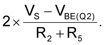
The “2” is due to the fact that R2 and R1 currents are identical (discounting the Early effect on Q1). The current through R1 is nearly constant regardless of the value of VGS. This current provides what U1 needs to operate.
The precision of the total DC current through the load is limited by the tolerances of R1 through R5, the U1 reference’s accuracy, and the value of the BJT’s temperature-dependent VBE drop. (U1’s maximum feedback reference current over its operating temperature is a negligible 1 µA.)
U1 requires a minimum of 100 µA to operate, so R5 is chosen to provide it with 150 µA. Per its On Semi datasheet, at this current and over Q1’s operating temperature range, the 2N3906’s typical VCE saturation voltage is 50 mV. Add that to the 15 mV drop across R1 for a total of 65 mV, which is the smallest achievable VSG value.
Accordingly, we are some small but indeterminant amount shy of the maximum drain current guaranteed for the part (at 25 °C, 25 V VDS, and 0 V VGS only) by its datasheet. At the other extreme, under otherwise identical conditions, a VGS of –3.5 V will guarantee a drain current of less than 10 µA. For such, U1 and the circuit as a whole will operate properly at a VS of 5 VDC.
Higher temperatures might require a more negative VGS by a maximum of –4.5 mV/°C and, therefore, possibly larger values of VS and, accordingly, of R5. This would be to ensure that U1’s cathode voltage remains above 1.24 V under all conditions.
D2 is selected for a Zener voltage which, when added to D1’s voltage drop, is greater than VS, but is less than the lesser of the maximum allowed cathode-anode voltage of U1 (18 V) and the maximum allowed VGS of M1 (20 V). D1‘s small capacitance shields the rest of the circuit from the Zener capacitance, which might otherwise induce oscillations. The diodes are probably not needed, but they provide cheap protection. Neither passes current or affects circuit performance during normal operation. C1 ensures stable operation.
U1 strives to establish a constant voltage at VS regardless of the DC and AC voltage variations of the unregulated supply V1. Working against it in descending order of impact are the magnitude of the conductance of the R3 + R4 resistor string, U1‘s falling loop gain with frequency, and M1’s large RDS and small CDS. Still, the circuit built around the 400-V VDS-capable M1 achieves some surprisingly good results in the test circuit of Figure 4.
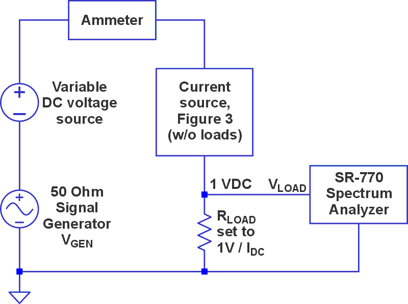 |
|
| Figure 4. | Circuit used to test the impedance of the Figure 3 current source. |
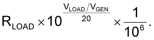
Figure 5 displays some measurements. Impedances in megohms are calculated using the formula
 |
|
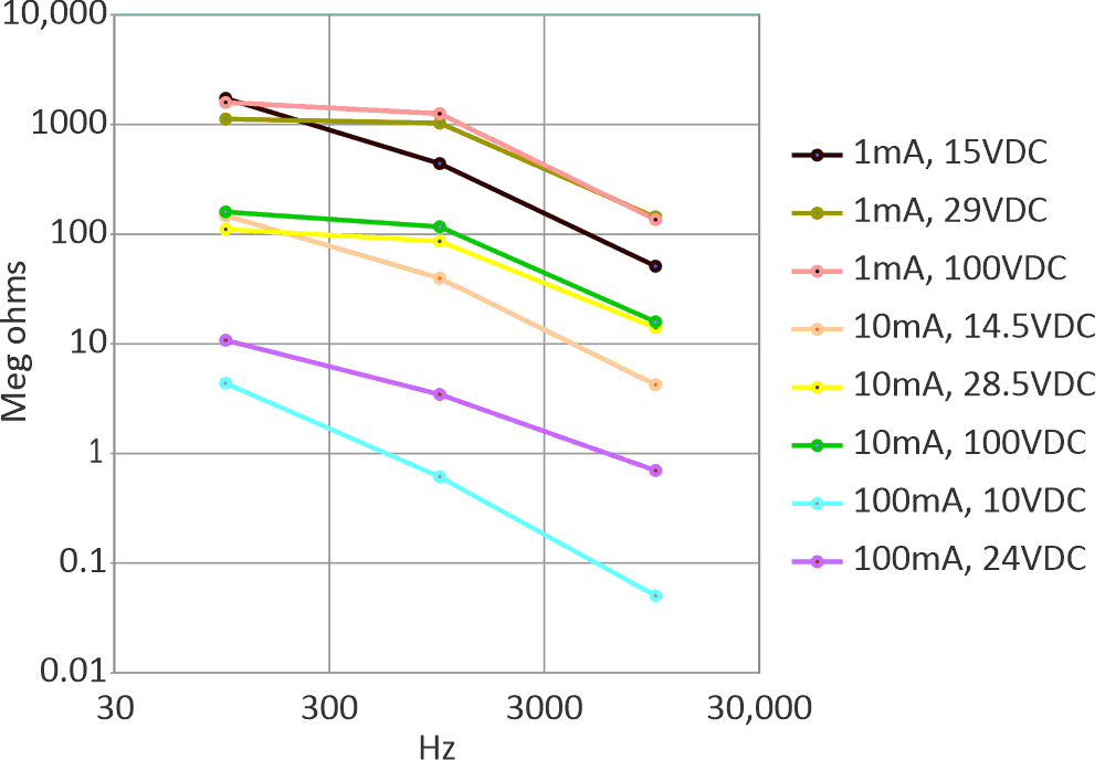
| Figure 5. | Plotted curves of Figure 3 current source impedance. |
Observations
There are several conclusions that can be drawn from the curves in Figure 5. The major one is that at low frequencies, the AC impedance Z is roughly inversely proportional to current. A more insightful way to express this is that Z is proportional to R3 + R4, which sets the current. With larger resistance, current variations produce larger voltages for the ‘431 IC to use for regulation; that is, there’s more gain available in the circuit’s feedback loop to increase impedance.
Another phenomenon is that in the 1 and 10-mA current curves, the impedance rises much more quickly as frequency increases above 1 kHz. This is consistent with the fact that the TLVH431B gain is more or less flat from DC to 1 kHz and falls thereafter. The following phenomenon masks this effect somewhat at the higher 100 mA current.
Finally, at all currents, there is an advantage to operating at higher values of VDS. This is especially apparent at the highest current, 100 mA. And this is consistent with the fact that for the characteristic curves of the DN2540 MOSFET seen in Figure 1, higher VDS voltages are required at higher currents before the curves become horizontal.
Precision current source
A precision high impedance, moderate-to high voltage-compliant current source has been introduced. Its two-terminal nature means that a load in series with it can be connected to the source’s positive or negative end. Unlike earlier designs, the ‘431 regulator IC’s operating current is independent of both the source’s supply voltage and of its MOSFET’s VGS voltage. The result is a more predictable DC current as well as higher AC impedances than would otherwise be obtainable.