Targeting use in portable-system applications that require raising a battery's voltage to a higher level, IC boost regulators often include output transistors that can drive storage inductors. However, most boost regulators' absolute-maximum input-voltage rating typically doesn't exceed 6 V, an adequate level for battery operation. In addition, breakdown voltage of the regulator's output transistor limits the regulator's absolute-maximum output voltage to 25 to 30 V, which may be too low for some applications.
You can extend a boost regulator's output-voltage range by adding an external transistor that has a higher breakdown voltage than the regulator. However, the internal design of a typical boost regulator's control circuitry often prevents direct drive of an external transistor's base or gate. As an alternative, you can add an external higher voltage transistor by connecting it in a cascode configuration.
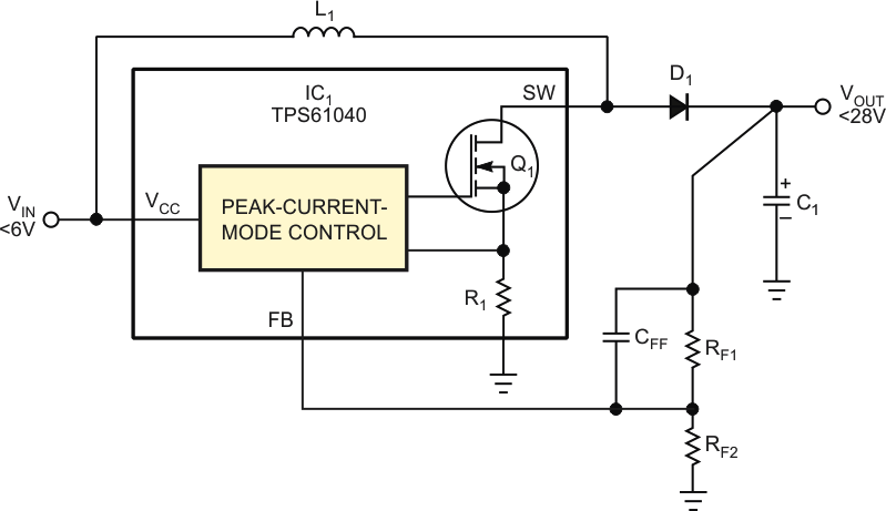
Most boost regulators feature a peak-current-control method that reduces the number of external components and thus shrinks the overall pc-board area of the converter circuit. Figure 1 shows a boost regulator based on a TPS61040 boost controller, IC1, which uses peak-current control.
 |
||
| Figure 1. | Based on the “barefoot” TPS61040, this dc/dc boost converter delivers output voltages only within IC1’s ratings. |
|
Applying input voltage VIN to IC1's VCC pin and to one leg of inductor L1 turns on IC1's internal MOSFET switch, Q1, allowing a gradually increasing amount of current to flow from VIN through L1, Q1, and internal current-sense resistor R1. The circuit's internal controller monitors the voltage across sense resistor R1 and, upon reaching a predetermined current limit, turns off Q1.
Interrupting the current through L1 raises the voltage across the inductor and applies forward bias to diode D1, which conducts and charges output capacitor C1 to a higher voltage than would be available from the input voltage alone. The input voltage, L1's inductance, and the preset peak current through R1 all affect Q1's on-time, and the output voltage sensed by IC1's FB (feedback) pin and its external components determines Q1's off-time. To maintain operation and set Q1's off-time, IC1's internal controller must monitor current through L1 using Q1 and R1.
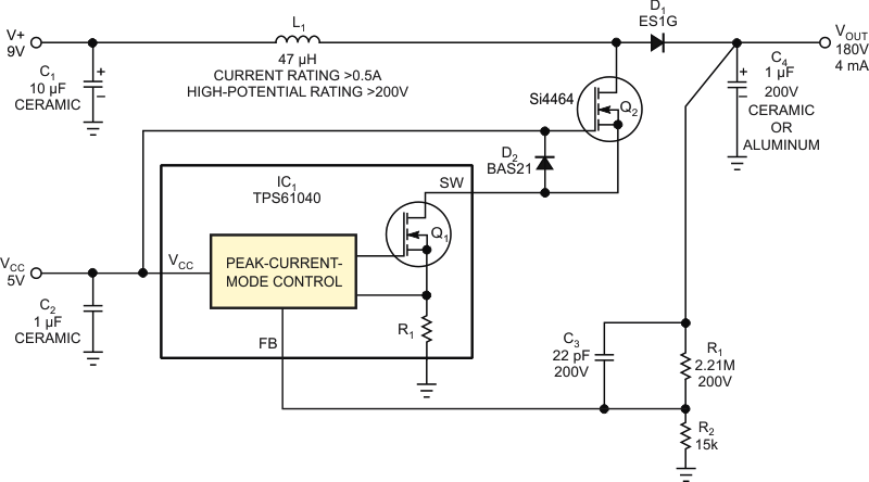
You can add a higher voltage MOSFET transistor, Q2 (Figure 2), for applications that require an output voltage higher than the internal transistor's breakdown voltage. To maintain the circuit's current-flow path through L1 and IC1's SW pin, you connect the external transistor in a cascode, or common-gate, configuration.
 |
||
| Figure 2. | Adding an external cascode-connected MOSFET transistor, Q2, with higher breakdown-voltage ratings, enables the circuit to produce higher output voltages. |
|
Q2 comprises a low-on-resistance, low-gate-voltage-threshold MOSFET with the addition of diode D2 between Q2's gate and source. To ensure the circuit's proper operation, VCC – 5 V in this example – must exceed Q2's gate-threshold turn-on voltage. In operation, IC1's internal control circuit turns on Q1, which pulls Q2's source close to ground level and turns on Q2 with almost 5 V of gate-to-source potential.
Current flows through inductor L1, external transistor Q2, internal transistor Q1, and sense resistor R1, and IC1's control circuit "sees" no difference with the installation of Q2. Once the inductor current reaches its preset limit, Q1 turns off, leaving Q2 with no path for current to flow from its source. The voltage on Q2's drain rises rapidly to the desired output voltage plus the voltage drop across D1. As the drain voltage rises, Q2's drain-to-source capacitance attempts to pull the MOSFET's floating source above 5 V, which forward-biases D2, connects IC1's SW pin voltage to 5 V plus one diode drop, and clamps Q2's source to the same voltage.
A boost converter delivers a 180 V output at 4 mA (VOUT) to bias a laser circuit from a 9 V power supply (V+). In this application, the 5 V input supply need provide only enough current – typically, a few milliamperes – to drive IC1's internal logic and the gate of cascode MOSFET Q2. You can use a dropping resistor and zener-diode voltage regulator (not shown) to supply the 5 V requirement from the 9 V supply. You can drive the inductor and IC1 from a common power supply or from a separate source that's within Q2's breakdown-voltage rating. The cascode circuit also can produce any output voltage that's within Q2's drain-to-source breakdown-voltage rating. Specify other components with an appropriate voltage rating – for example, breakdown-voltage ratings of inductor L1 and capacitor C1 should safely exceed the desired output voltage.