Fabien Dubois
EDN
The circuit in this Design Idea lets you set a well-controlled voltage rate of change, often expressed as the differential dV/dt (instantaneous rate of voltage change over time in volts per second). You can vary the sensitivity with a potentiometer. Set the dV/dt from 1 V/200 nsec to 1 V/3 msec. The input voltage can range from a few volts to 30 V. Higher-voltage transistors can be used to increase the upper voltage limit. The circuit precharges a capacitor with a slow and controllable dV/dt to avoid a large inrush current during power-up. You can also use the circuit to create a high dV/dt for susceptibility testing on other circuits.
 |
||
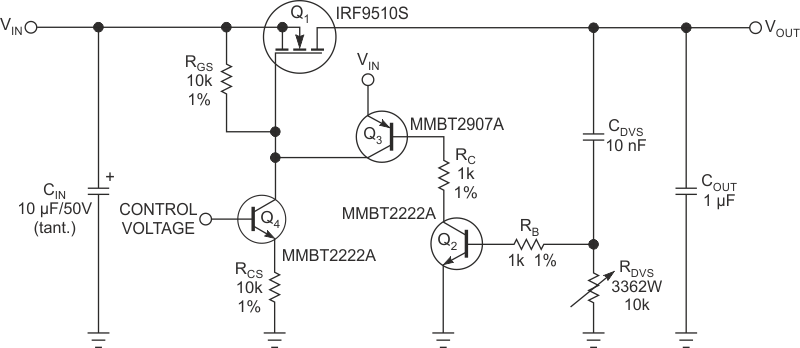
| Figure 1. | This circuit creates a fixed dV/dt based on the control voltage and the setting of RDVS. | |
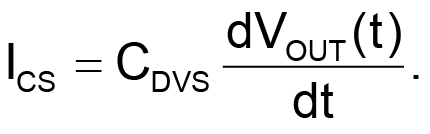
The circuit uses a P-channel MOSFET, Q1, to control the rate of change of the output voltage (Figure 1). You drive the MOSFET with a constant-current source comprising Q4 and RCS, which feeds gate-to-source resistor RGS. Applying a positive control voltage to the base of Q4 draws a current that creates a voltage across RGS. This voltage occurs across the gate and source of Q1, turning it on. The circuit uses capacitor CDVS as a sensing device of the rate of change of the output voltage. Voltage variations across CDVS generate a current that creates a current proportional to the dV/dt, as the following equation shows:
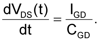
Resistor RDVS converts this current into a voltage signal. When that voltage reaches approximately 0.67 V, it turns on Q2, which turns on Q3. The current that Q3 supplies from the input tends to lower the Q1 gate-to-source voltage and reduces its drive. You use RB to limit the base current of Q2. This servo action puts the gate-to-source voltage of the MOSFET in the Miller plateau, a constant-current region of the FET’s characteristic curve. The FET has an internal Miller capacitance, CGD, between the gate and the drain pins. The circuit’s constant-current source controls the charge current of this Miller capacitance. As transistor Q3 injects current to the gate, Miller current IGD decreases and the slope of the output voltage decreases accordingly, as the following equation shows:
The feedback loop keeps the dV/dt ratio constant. The rate of change of the output voltage is a function of the base-emitter voltage of Q2, RDVS, and CDVS, as the following equation shows: