When designing logic for higher-than-usual supply voltages, such as 24 V, you can use a voltage regulator with a standard logic family and interface it through level shifters. Alternatively, if the logic is not too complex and the speed is not extensively high, you can build gates from discrete components and operate them directly from the available voltage. Discrete-component AND, OR, and NOT functions are relatively straightforward, but XOR and XNOR functions usually require combining several of the basic AND, OR, and NOT functions.
This Design Idea presents an unusual method of performing the exclusive functions with two resistors, four diodes, and one transistor. The NPN configuration results in the XNOR operation, and the PNP configuration gives the XOR operation.
 |
||
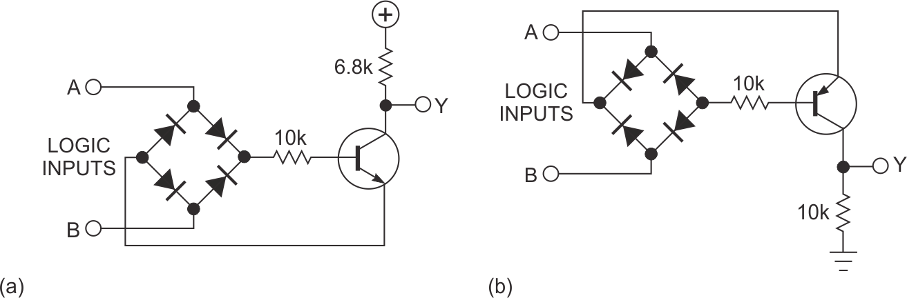
| Figure 1. | Discrete implementations of XNOR (a) and XOR operations (b) allow you to run logic at higher supply voltages than standard logic families. |
|
Consider the XNOR circuit in Figure 1a. When either of the gate inputs, A or B, is at an opposite logic state, a voltage drop of the high voltage minus the low voltage minus 1.2 V is available to forward-bias the base-emitter junction. The transistor turns on, and the logic-zero voltage at the collector is approximately
0.6 + VL + VCE,
where VL is the low voltage and VCE is the collector-to-emitter voltage. When inputs A and B are at the same logic state, you cannot forward-bias the transistor’s base-to-emitter junction, so output Y is at the supply voltage.
The choice of 6.8 kΩ at the collector is based on driving the A and the B inputs with standard transistor-transistor or CMOS logic, and you can change it to suit your application. The CMOS 4000 family can reliably source or sink 1 mA with a 5 V supply. Low-speed TTL can source 0.4 mA and sink 8 mA. A 0.4-mA logic-one drive is sufficient for the base current, but the logic zero at either A or B forms the emitter current and is of more concern with regard to the limited 1-mA sink of the CMOS. With a net 1-mA current and approximately 250 μA remaining for the output load, you must choose a 6.8-kΩ resistor (0.75 mA × 6.8 kΩ) to drop approximately 5 V.
Next, consider the XOR configuration in which logic zero at either A or B is relevant for the base and logic one is relevant for the emitter. The logic-one voltage available at Y is
VH – 0.6 В – VCE,
and logic zero is approximately 0 V but current-limited through the collector resistor.
The concern here is with the TTL logic-one output current of approximately 0.4 mA, which is the transistor’s emitter current. With the choice of 10 kΩ for the collector resistor, the voltage drop across it can reach nearly 4 V. This level would be tolerable for driving CMOS loads but not for TTL, which demands a current of at least 0.4 mA for logic-zero inputs when Y is at logic zero. The 10-kΩ resistor cannot provide this current. However, using the previous XNOR configuration and another inverting transistor after Y, you can obtain the XOR function (Figure 1b). The XOR seems to be suitable only for the CMOS/TTL input at A and B and capable of driving only CMOS at output Y.