Professional-audio equipment commonly uses Analog Devices‘ high-performance, quad-voltage-controlled SSM2164 attenuator. The control response is –30 dB/V, with 0 V producing unity gain. Attenuation increases as the applied control voltage increases in the positive direction. The circuit in Figure 1 extends the range of applications for this versatile chip by providing a simple means of linearizing the control response. The result is an amplifier with gain directly proportional to the control voltage. In addition, the circuit also functions as a simple logarithm generator. You can use a single SSM2164 to make two high-quality, linear voltage-controlled amplifiers using this method. The four gain cells in the SSM2164 are tightly matched, current-in, current-out transconductance multipliers. The control response of each gain cell is:
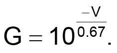
The cells are noninverting structures.
 |
||
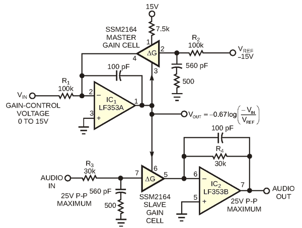
| Figure 1. | You can obtain both a gain-controlled output and a logarithmic output using this configuration. | |
Each voltage-controlled amplifier uses two gain cells. A “master” cell in the feedback loop of an op amp generates a logarithmic voltage output in response to a linear voltage input. This log voltage then goes to the control pin of the second (matching) “slave” cell, which processes the audio signal. Op amp IC1 maintains its inverting input at virtual ground by servo-controlling the gain of the master SSM2164 cell, which connects to the negative reference voltage. The output of IC1 is a logarithmic function of the input:
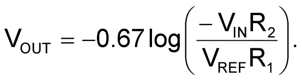
VIN is the gain-control voltage, and VREF is the negative reference voltage. VOUT then drives the control pin of the slave cell. Substituting the expression for VOUT for V in the expression for gain yields the following:
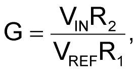
which is the desired linear response.
Op amp IC2 converts the slave cell’s output current to an audio voltage with a gain of R4/R3. The overall expression for the gain is:
If R1 = R2 and R3 = R4, the expression reduces to:
and
Setting VIN to 15 V and VREF to –15 V produces unity gain with the indicated component values. The gain decreases smoothly to –70 to –80 dB as the control voltage decreases (Figure 2). The voltage-controlled amplifier then shuts off completely (attenuation=100 dB) when the control voltage drops to within a few millivolts of 0 V. Negative voltages make the output of IC1 swing close to the positive rail, but IC1 promptly comes off the rail when the control voltage returns to the 0 to 15 V range. The circuit produces no audible clicks and works well at lower supply voltages, such as ±5 V.
 |
||
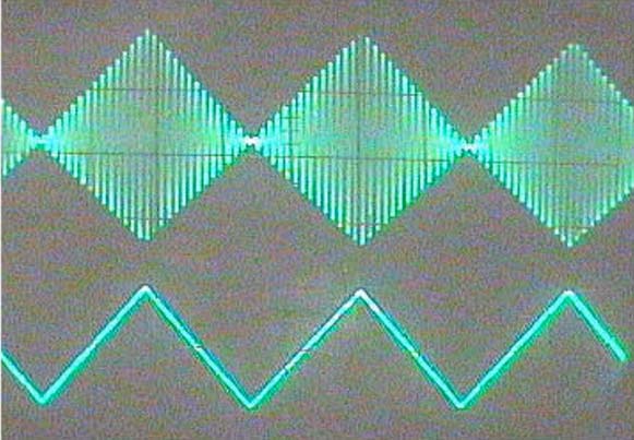
| Figure 2. | The lower trace is a 0 to 3 V triangle wave, which you use to modulate the 10-kHz sine wave in the upper trace. Note the linear modulation envelope. |
|
For best performance, IC1 should be a low-offset, low-input-current unit, and IC2 should be a high-quality, low-noise audio op amp. However, you can obtain reasonably good performance with inexpensive op amps, such as the TL072 and LF353. The prototype unit achieved a control range of 75 to 80 dB, using an OP290 for IC1. The control-voltage feedthrough on the audio output is minimal, varying 10 to 20 mV when you sweep the gain through a 70-dB range. The noise and distortion performance is excellent, because the design uses the gain cells in the standard configuration in the SSM2164 data sheet.